Polycrystalline gallium-nitride self-supporting substrate and light-emitting element using same

A gallium nitride and gallium nitride-based technology, applied in the field of polycrystalline gallium nitride self-supporting substrates, can solve the problems of inability to form electrodes, prone to dislocations, inconsistent lattice constants and thermal expansion rates, etc.

Active Publication Date: 2016-05-04
NGK INSULATORS LTD
View PDF8 Cites 5 Cited by
  • Summary
  • Abstract
  • Description
  • Claims
  • Application Information

AI Technical Summary

Problems solved by technology

[0003] However, when a GaN layer is formed on a sapphire substrate, dislocations tend to occur because the lattice constant and thermal expansion coefficient of the GaN layer and sapphire, which is a different substrate, do not match.
In ...

Method used


Image

  • Polycrystalline gallium-nitride self-supporting substrate and light-emitting element using same
  • Polycrystalline gallium-nitride self-supporting substrate and light-emitting element using same
  • Polycrystalline gallium-nitride self-supporting substrate and light-emitting element using same

Examples


Embodiment Construction

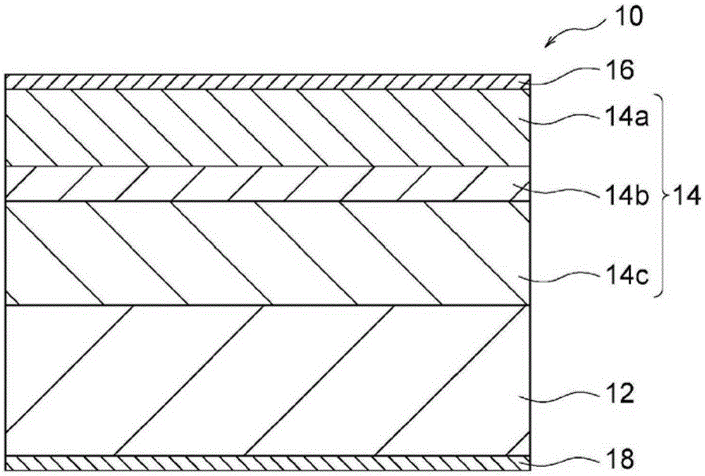
[0016] Polycrystalline Gallium Nitride Free-standing Substrate

[0017] The gallium nitride substrate of the present invention may have the form of a self-supporting substrate. The "self-supporting substrate" in the present invention refers to a substrate that can be handled or used as a solid object without deforming or breaking due to its own weight during handling or use. The polycrystalline gallium nitride self-supporting substrate of the present invention can be used as a substrate of various semiconductor devices such as a light-emitting element, and can also be used as an electrode (which can be a p-type electrode or an n-type electrode), a p-type layer, an n-type electrode, etc. Parts or layers other than base materials such as molded layers. It should be noted that in the following description, the advantages of the present invention are described by taking light-emitting elements as one of the main applications as an example, but the same or similar advantages are...


PUM

PropertyMeasurementUnit
Thicknessaaaaaaaaaa
Particle sizeaaaaaaaaaa
Thicknessaaaaaaaaaa

Abstract

This invention provides a polycrystalline gallium-nitride self-supporting substrate comprising a plurality of gallium-nitride-based single-crystal grains aligned to a specific crystal orientation in a direction that is substantially parallel to the normal direction. The crystal orientations of said gallium-nitride-based single-crystal grains, as measured by subjecting the surface of the self-supporting substrate to electron backscatter diffraction (EBSD) and performing inverse-pole-figure mapping, form a variety of angles with the aforementioned specific crystal orientation, and the mean value of the distribution of said angles is between 1degrees and 10 degrees, inclusive. This light-emitting element comprises the abovementioned self-supporting substrate and a light-emitting functional layer that is formed on top of the substrate and contains one or more layers each comprising a plurality of semiconductor single-crystal grains each exhibiting a single-crystal structure that is substantially parallel to the normal direction. This invention makes it possible to provide a polycrystalline gallium-nitride self-supporting substrate with a reduced defect density in the surface thereof. A light-emitting element that uses said polycrystalline gallium-nitride self-supporting substrate and exhibits a high luminous efficacy can also be obtained.

Description

technical field [0001] The present invention relates to a polycrystalline gallium nitride self-supporting substrate and a light emitting element using the polycrystalline gallium nitride self-supporting substrate. Background technique [0002] As a light-emitting device such as a light-emitting diode (LED) using a single crystal substrate, a light-emitting device in which various gallium nitride (GaN) layers are formed on sapphire (α-alumina single crystal) is known. For example, mass production of products having a structure in which an n-type GaN layer, a multi-quantum well layer (MQW), and a p-type GaN layer are sequentially stacked on a sapphire substrate has begun. Layered quantum well layers and barrier layers including GaN layers are stacked alternately. In addition, laminated substrates suitable for such applications have also been proposed. For example, Patent Document 1 (Japanese Unexamined Patent Application Publication No. 2012-184144) proposes a gallium nitrid...

Claims


Application Information

Patent Timeline
IPC IPC(8): H01L33/16C30B29/38H01L33/32
CPCH01L33/16H01L33/32C30B9/12C30B19/02C30B19/12C30B25/18C30B28/04C30B29/406C30B29/605C30B29/28H01L33/12H01L2924/12041
Inventor 渡边守道吉川润仓冈義孝七泷努
Owner NGK INSULATORS LTD
Why Eureka
Try Eureka