Light emitting diode chip with inverted structure and fabrication method of light emitting diode chip

A light-emitting diode and chip technology, which is applied in the direction of electrical components, circuits, semiconductor devices, etc., can solve the problems of low luminous efficiency and poor current expansion, and achieve the improvement of luminous efficiency and luminous intensity, the reduction of forward voltage, and the uniform distribution of current density Effect

Active Publication Date: 2016-05-25
HC SEMITEK SUZHOU
View PDF7 Cites 7 Cited by
  • Summary
  • Abstract
  • Description
  • Claims
  • Application Information

AI Technical Summary

Problems solved by technology

[0006] In order to solve the problems of poor current expansion and low luminous efficiency in the prior art, an embodiment of the present invention provides a light-emitting diode chip with a flip-chip structure and a preparation method thereof

Method used


Image

  • Light emitting diode chip with inverted structure and fabrication method of light emitting diode chip
  • Light emitting diode chip with inverted structure and fabrication method of light emitting diode chip
  • Light emitting diode chip with inverted structure and fabrication method of light emitting diode chip

Examples


Embodiment 1

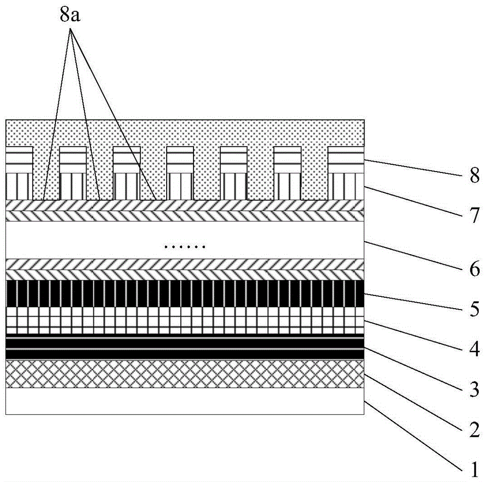
[0030] An embodiment of the present invention provides a light-emitting diode chip with a flip-chip structure, see figure 1 , the LED chip includes a substrate 1, and a P-type current spreading layer 2, a P-type confinement layer 3, an active layer 4, an N-type confinement layer 5, and an N-type current spreading layer 6 stacked on the substrate 1 in sequence. The LED chip also includes an N-type ohmic contact layer 7, a P-type ohmic contact layer 8 and a transparent conductive layer 9 stacked on the N-type current spreading layer 6, and the P-type ohmic contact layer 8 and the N-type ohmic contact layer 7 are GaAs The transparent conductive layer 9 is an Indium Tin Oxides (ITO for short) layer, and the P-type ohmic contact layer 8 and the N-type ohmic contact layer 7 are provided with a plurality of through holes 8a extending to the N-type current spreading layer 6 .

[0031] In this embodiment, the substrate 1 is a Si substrate or a sapphire substrate, the P-type current spr...

Embodiment 2

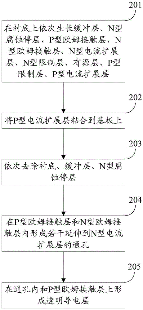
[0048] The embodiment of the present invention provides a method for preparing a light-emitting diode chip, which is suitable for preparing the light-emitting diode chip provided in Example 1, see figure 2 , the preparation method comprises:

[0049] Step 201: sequentially growing a buffer layer, an N-type corrosion stop layer, a P-type ohmic contact layer, an N-type ohmic contact layer, an N-type current spreading layer, an N-type confinement layer, an active layer, a P-type confinement layer, P-type current spreading layer.

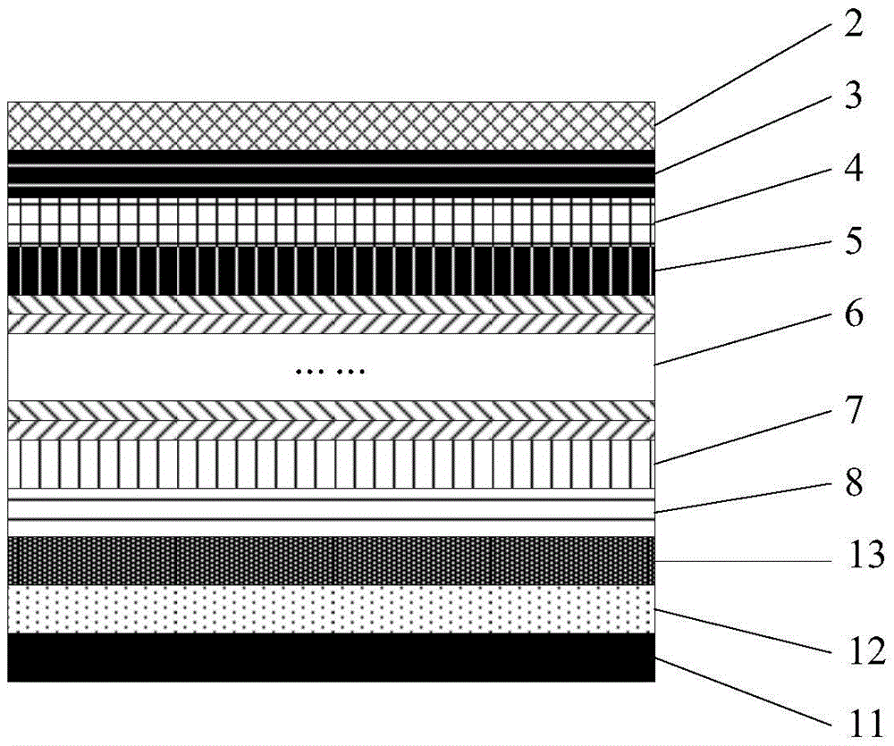
[0050] Figure 3a It is a schematic structural diagram of the LED chip after step 201 is performed. Among them, 11 is the substrate, 12 is the buffer layer, 13 is the N-type corrosion stop layer, 8 is the P-type ohmic contact layer, 7 is the N-type ohmic contact layer, 6 is the N-type current spreading layer, 5 is the N-type confinement layer , 4 is an active layer, 3 is a P-type confinement layer, and 2 is a P-type current spreading layer.

[0051...


PUM


Abstract

The invention discloses a light emitting diode chip with an inverted structure and a fabrication method of the light emitting diode chip, belonging to the technical field of a semiconductor. The light emitting diode chip comprises a substrate and a P-type current extension layer, a P-type limiting layer, an active layer, an N-type limiting layer, an N-type current extension layer, an N-type ohmic contact layer, a P-type ohmic contact layer and a transparent conductive layer which are sequentially laminated on the substrate, wherein the P-type ohmic contact layer and the N-type ohmic contact layer are GaAs layers, the transparent conductive layer is an indium tin oxide (ITO) layer, and a plurality of through holes are formed in the P-type ohmic contact layer and the N-type ohmic contact layer and extend to the N-type current extension layer. With the adoption of the ITO transparent conductive layer, current extension is achieved, the extended current is injected into the N-type current extension layer through the ohmic contact layers, so that the current is extended very well, the current density distribution is uniform, and the luminous efficiency and the luminous intensity are improved.

Description

technical field [0001] The invention relates to the technical field of semiconductors, in particular to a light-emitting diode chip with a flip-chip structure and a preparation method thereof. Background technique [0002] In recent years, AlGaInP light-emitting diodes (Light Emiting Diodes, LEDs for short) with high luminance characteristics have been widely used in more and more application fields, and the market demand is constantly expanding. [0003] The AlGaInP LED chip includes a substrate, an N-type current spreading layer, an N-type confining layer, an active layer, a P-type confining layer, and a P-type current spreading layer from bottom to top, and the N-type current spreading layer is an N-type AlGaInP layer. [0004] In the process of realizing the present invention, the inventor finds that there are at least the following problems in the prior art: [0005] N-type AlGaInP material has poor current spreadability, resulting in uneven current density distributio...

Claims


Application Information

Patent Timeline
Patent Type & Authority Applications(China)
IPC IPC(8): H01L33/36H01L33/38H01L33/00
CPCH01L33/36H01L33/38H01L33/382H01L2933/0016
Inventor 邢振远李彤王世俊董耀尽
Owner HC SEMITEK SUZHOU
Why Eureka
Try Eureka