Algan template, preparation method of algan template and semiconductor device on algan template

A technology of semiconductors and nitride semiconductors, applied in semiconductor devices, electrical components, circuits, etc., can solve the problems of uneven growth temperature of quantum well structures, inability to mass-produce high-yield epitaxial wafers, and poor wavelength uniformity of epitaxial wafers. Optimizing wavelength uniformity, achieving feasibility, and reducing the effect of accumulated stress

Active Publication Date: 2018-10-09
HC SEMITEK SUZHOU
View PDF3 Cites 0 Cited by
  • Summary
  • Abstract
  • Description
  • Claims
  • Application Information

AI Technical Summary

Problems solved by technology

[0005] In order to solve the problem that when GaN epitaxy is grown on the existing AlN template, the subsequent GaN epitaxy will accumulate relatively large stress, and the epitaxial wafer is in a warped state when growing the quantum well structure in GaN epitaxy, so that the growth temperature of the quantum well structure is not stable. Uniformity, poor wavelength uniformity of epitaxial wafers, resulting in the inability to mass-produce high-yield epitaxial wafers. Embodiments of the present invention provide an AlGaN template, a method for preparing an AlGaN template, and a semiconductor device on an AlGaN template.

Method used


Image

  • Algan template, preparation method of algan template and semiconductor device on algan template
  • Algan template, preparation method of algan template and semiconductor device on algan template
  • Algan template, preparation method of algan template and semiconductor device on algan template

Examples


Embodiment Construction

[0032] In order to make the object, technical solution and advantages of the present invention clearer, the implementation manner of the present invention will be further described in detail below in conjunction with the accompanying drawings.

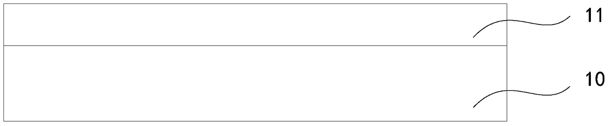
[0033] figure 2 It shows an AlGaN template provided by the first embodiment of the present invention, such as figure 2 As shown, the AlGaN template includes a substrate 10 and Al deposited on the substrate 10 1-x Ga x N crystal thin film 11, 0

[0034] Wherein, the present embodiment does not limit the type of the substrate 10, and the substrate 10 may be Si, SiC, sapphire, ZnO, GaAs, GaP, MgO, Cu, W or SiO 2 substrate.

[0035] In realization, the Al can be deposited on the substrate by a physical vapor deposition (English: Physical Vapor Deposition, abbreviation: PVD) process or an electron beam evaporation process. 1-x Ga x N crystalline film 11. When adopting PVD process to deposit this Al on the substrate 10 1-x Ga ...


PUM


Abstract

The invention discloses an AlGaN template, a preparation method of the AlGaN template and a semiconductor device on the AlGaN template, belonging to the technical field of semiconductors. The AlGaN template includes: a substrate and an Al1‑xGaxN crystalline film deposited on the substrate, 0

Description

technical field [0001] The invention relates to the technical field of semiconductors, in particular to an AlGaN template, a preparation method of the AlGaN template and a semiconductor device on the AlGaN template. Background technique [0002] Currently, most GaN-based blue light emitting diodes (English: light emitting diode, abbreviation: LED) and GaN-based white light LEDs use sapphire substrates. Since sapphire and GaN materials have always had lattice mismatch and thermal mismatch problems, and there is only a small lattice mismatch between AlN materials, GaN materials, and sapphire substrates, AlN is placed on the sapphire substrate as a buffer layer and GaN. Specifically, an AlN buffer layer is first grown on a sapphire substrate to make an AlN template, and then GaN epitaxy is grown on the AlN template to make an LED epitaxial wafer. [0003] In the process of realizing the present invention, the inventor finds that there are at least the following problems in th...

Claims


Application Information

Patent Timeline
Patent Type & Authority Patents(China)
IPC IPC(8): H01L33/00
CPCH01L33/0075H01L33/12H01L33/007H01L33/32
Inventor 董彬忠张武斌艾海平李鹏王江波
Owner HC SEMITEK SUZHOU
Why Eureka
Try Eureka