Method for growing active area epitaxial wafer of nanometer folded structure

A technology of active regions and epitaxial wafers, applied in the fields of electrical components, semiconductor/solid-state device manufacturing, circuits, etc., can solve problems such as reducing internal quantum efficiency

Inactive Publication Date: 2010-09-01
INST OF SEMICONDUCTORS - CHINESE ACAD OF SCI
View PDF2 Cites 0 Cited by
  • Summary
  • Abstract
  • Description
  • Claims
  • Application Information

AI Technical Summary

Problems solved by technology

The presence of a polarizing electric field in a quantum well is also a factor that reduces the internal quantum efficiency

Method used


Image

  • Method for growing active area epitaxial wafer of nanometer folded structure
  • Method for growing active area epitaxial wafer of nanometer folded structure
  • Method for growing active area epitaxial wafer of nanometer folded structure

Examples


Embodiment 1

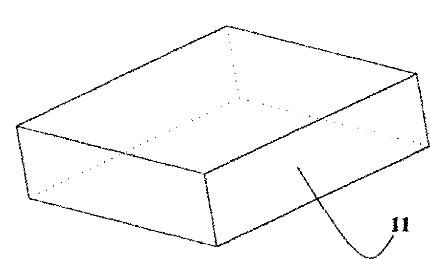
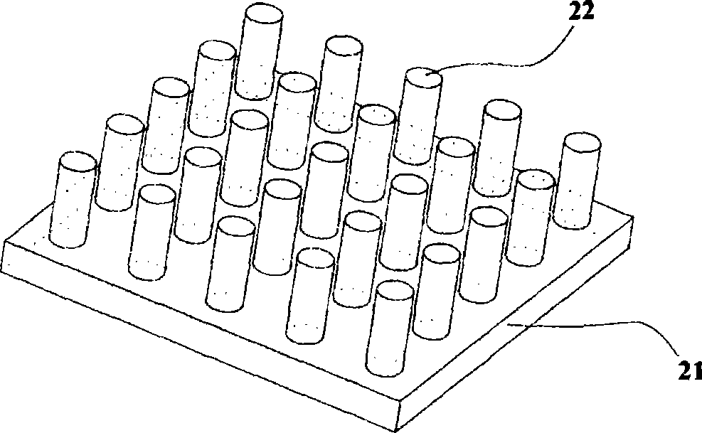
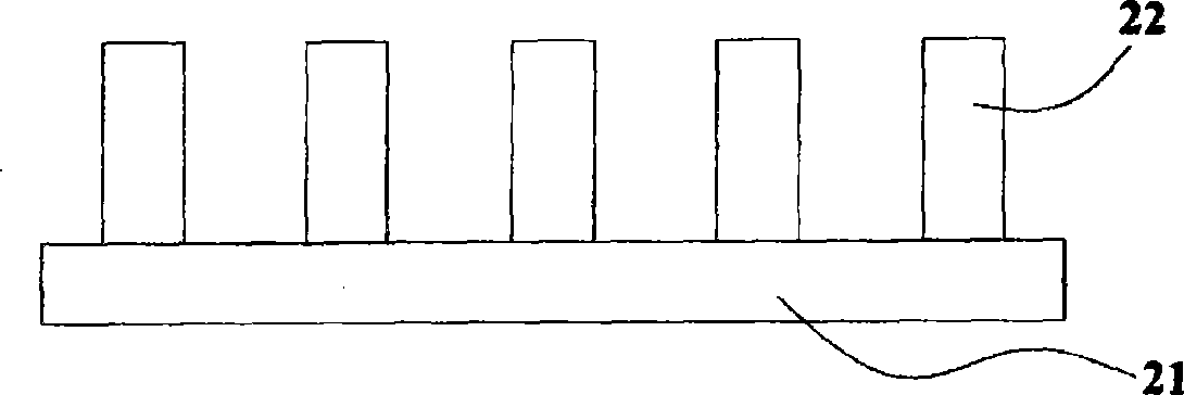
[0033] Embodiment one: see figure 1 - Figure 4. First prepare and obtain an AlInGaN material template 11; then prepare 1-1000 nanometer thick SiO on the AlInGaN material template by chemical vapor deposition method 2 、SiN x Dielectric film; then a layer of metal is deposited on the dielectric film, and the metal is aggregated into metal islands with a diameter of about 10-200 nanometers by rapid annealing. Using the metal island as a mask material, the AlInGaN material template is etched by ion beam etching and coupled plasma etching, thereby making an AlInGaN nano-column array 21, the nano-column array 21 includes a plurality of nano-columns 22; and then AlInGaN An active region layer 31 with a nanofold structure is grown on the nanocolumn array 21 and nanocolumn 22, and finally a p-type GaN layer 41 with a nanohole array 42 is grown on the active region layer 31 with a nanofold structure to obtain a LED epitaxial wafer with nanofold structure active region;

Embodiment 2

[0034] Embodiment two: see figure 1 - Figure 4. First prepare and obtain an AlInGaN material template 11; then prepare 1-1000 nanometer thick SiO on the AlInGaN material template by chemical vapor deposition method 2 、SiN x The dielectric film; then use the method of holographic exposure and electron beam exposure to make template pattern on the dielectric film; finally use ion beam etching and coupled plasma etching method to etch the AlInGaN material template, so as to make the AlInGaN nano column array 21, the The nanocolumn array 21 includes a plurality of nanocolumns 22; then an active region layer 31 with a nanofold structure is grown on the AlInGaN nanocolumn array 21 and the nanocolumn 22, and finally a belt is grown on the active region layer 31 with a nanofold structure. A p-type GaN layer 41 with a nanohole array 42 to obtain an LED epitaxial wafer with a nanofold structure active region;

Embodiment 3

[0035] Embodiment three: see figure 1 - Figure 4. First prepare and obtain an AlInGaN material template 11; then use laser scanning etching technology to etch the AlInGaN material template to make an AlInGaN nano-column array 21, the nano-column array 21 includes a plurality of 22; then the AlInGaN nano-column array 21 and nano An active region layer 31 with a nanofold structure is grown on the pillar 22, and finally a p-type GaN layer 41 with a nanohole array 42 is grown on the active region layer 31 with a nanofold structure to obtain an active region with a nanofold structure LED epitaxial wafers;

[0036] Use case one: first see figure 1 -As shown in Figure 4, a layer of 1-10 micron thick n-type AlInGaN epitaxial layer is epitaxially grown on a sapphire substrate by metal organic chemical vapor deposition (MOCVD), wherein the composition values ​​of Al, In and Ga can be adjusted is any value between 0-1, and the AlInGaN material template 11 is obtained. Secondly, the A...


PUM


Abstract

The invention discloses a method for growing active area epitaxial wafer of nanometer folded structure, which is characterized in that the method comprises the following steps: 1. an AlxInyGazN material template is prepared, wherein, x+y+z=1, and x, y and z are not smaller than 0 and not bigger than 1; 2. nanometer processing technology is used to produce an AlInGaN nanorod array on the AlxInyGazN material template, and the AlInGaN nanorod array comprises a plurality of AlInGaN nanorods; 3. An active area layer with nanometer folded structure is grown on the upper surface of the AlInGaN nanorod array, the AlInGaN nanorods and the AlInGaN nanometer material template; 4. a p-type GaN layer with a nano-porous array is grown on the active area layer with nanometer folded structure; the production of epitaxial wafers is finished when the gap of the AlInGaN nanorod array is completely filled with the p-type GaN layer.

Description

technical field [0001] The invention relates to a method for preparing a novel light-emitting diode active region structure and an epitaxial wafer with such a grievous structure, in particular to a nano-pillar array structure prepared on a substrate template by using nano-processing technology, and then the nano-pillar A method for preparing the active region of a light-emitting diode by growing the top surface and the side surface, and finally obtaining a light-emitting diode epitaxial wafer with a nano-folded structure active region. Background technique [0002] Liquid crystal displays with light-emitting diode (LED) backlights have gradually entered the market of small and medium-sized displays such as notebook computers and desktop computers, and have opened up a large market for high-power red, green, blue and white LEDs in addition to semiconductor lighting. high-end applications. However, in order to further meet the needs of high-end applications such as display sc...

Claims


Application Information

Patent Timeline
Patent Type & Authority Patents(China)
IPC IPC(8): H01L21/20H01L33/00H01L21/02
Inventor 朱建军
Owner INST OF SEMICONDUCTORS - CHINESE ACAD OF SCI
Why Eureka
Try Eureka