LED chip electrode, LED chip structure and fabrication methods of LED chip electrode and LED chip structure

An LED chip and manufacturing method technology, applied in circuits, electrical components, semiconductor devices, etc., can solve problems such as failure of light-emitting diodes, decreased luminous efficiency, abnormal light decay, etc., to increase migration rate, save manufacturing costs, and simplify process flow Effect

Inactive Publication Date: 2016-06-01
XIAMEN SANAN OPTOELECTRONICS TECH CO LTD
View PDF9 Cites 7 Cited by
  • Summary
  • Abstract
  • Description
  • Claims
  • Application Information

AI Technical Summary

Problems solved by technology

Light-emitting diodes with this structure tend to have abnormal light decay problems during package aging, especially in high-temperature and high-humidity environments, where metal reflective layers such as Al or Ag are unstable and are more likely to interact with elements such as Cl and O in the environment. Oxidation due to the reaction, resulting in a decrease in light efficiency, electrode bubbling, peeling and even electrode drop, which leads to the failure of the light-emitting diode

Method used


Image

  • LED chip electrode, LED chip structure and fabrication methods of LED chip electrode and LED chip structure
  • LED chip electrode, LED chip structure and fabrication methods of LED chip electrode and LED chip structure
  • LED chip electrode, LED chip structure and fabrication methods of LED chip electrode and LED chip structure

Examples


Embodiment 1

[0053] A light emitting diode with wrapped electrodes is prepared through the following process steps.

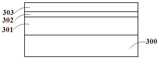
[0054] Such as image 3 As shown, a substrate is provided, and the substrate can be a substrate or a light-emitting epitaxial layer or a combination of the two. In this implementation, the preferred substrate is a sapphire substrate; on the sapphire substrate 300, metal organic compound chemical vapor deposition (English Abbreviated as MOCVD) light-emitting epitaxial layer, which sequentially includes an N-type layer 301 , a light-emitting layer 302 , and a P-type layer 303 from bottom to top.

[0055] Such as Figure 4 As shown, in the light-emitting epitaxial layer, a partially exposed N-type layer 301 is etched downward from the surface of the P-type layer 303 by using a mask and dry etching technology.

[0056] Such as Figure 5 As shown, a current spreading layer 304 is formed on the surface of the P-type layer 303 of the light-emitting epitaxial layer material, and...

Embodiment 2

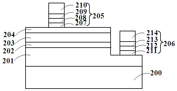
[0063] Such as Figure 10 As shown, the difference from Embodiment 1 is that the reflective structure of this embodiment is formed by sputtering, that is, the metal reflective layers 407 and 412, the first metal isolation layers 408 and 413, and the second metal isolation layer 409 are sequentially sputtered. The metal reflective structure composed of 414 and 414, the sides of each structural layer are inclined, and the cross-sectional view of the metal reflective structure is a trapezoidal shape with a narrow top and a wide bottom, so that the metal surface layer formed by the subsequent ion source plating method is better coated on the metal reflector. Structurally, the contact between the oxidant and the metal Al or Ag in the reflective structure is isolated, and good coating can also alleviate the migration and precipitation of the metal Al or Ag, thereby further improving the reliability of the light emitting diode.


PUM


Abstract

The invention discloses an LED chip electrode, an LED chip structure and fabrication methods of the LED chip electrode and the LED chip structure. The fabrication method of the LED chip electrode comprises the following steps: forming a negative photoresist on a substrate, defining an electrode pattern and removing the negative photoresist in a pattern region to form an electrode window; forming a reflecting structure on the electrode window; and forming a metal surface layer on the reflecting structure by an ion source-assisted plating method and finishing coating the top surface and the side walls of the reflecting structure. Therefore, the coating range of the reflecting structure is increased; the technological process is effectively simplified; the fabrication cost is saved; and the method is suitable for large-scale production. In further, the metal surface layer is formed by the ion source-assisted plating method to prepare an electrode structure which is compact, small in internal stress and smooth in surface. Therefore, the reliability of an LED is improved.

Description

technical field [0001] The invention relates to the field of semiconductor devices, in particular to an LED chip electrode and chip structure and a manufacturing method thereof. Background technique [0002] Light Emitting Diode (English for LightEmittingDiode, referred to as LED) is a semiconductor diode, it can convert electrical energy into light energy, emit yellow, green, blue and other colors of visible light and infrared and ultraviolet invisible light. Compared with small incandescent bulbs and neon lamps, it has the advantages of low operating voltage and current, high reliability, long life and convenient adjustment of luminous brightness. Since the gallium nitride (GaN)-based LED was successfully developed in the 1990s, with the continuous progress of research, its luminous brightness has also been continuously improved, and its application fields have become wider and wider. [0003] refer to figure 1 As shown, in the current conventional front-mount light-emit...

Claims


Application Information

Patent Timeline
Patent Type & Authority Applications(China)
IPC IPC(8): H01L33/00H01L33/38H01L33/40
CPCH01L33/007H01L33/38H01L33/405H01L2933/0016
Inventor 夏章艮林素慧彭康伟洪灵愿黄禹杰徐宸科
Owner XIAMEN SANAN OPTOELECTRONICS TECH CO LTD
Why Eureka
Try Eureka