

Method for preparing GaN/conductive substrate composite material by magnetron sputtering method and application of GaN/conductive substrate composite material on lithium ion battery
A composite material and magnetron sputtering technology, applied in battery electrodes, secondary batteries, circuits, etc., can solve problems that have not been reported
- Summary
- Abstract
- Description
- Claims
- Application Information
AI Technical Summary
Problems solved by technology
Method used
Image

Examples
Embodiment 1
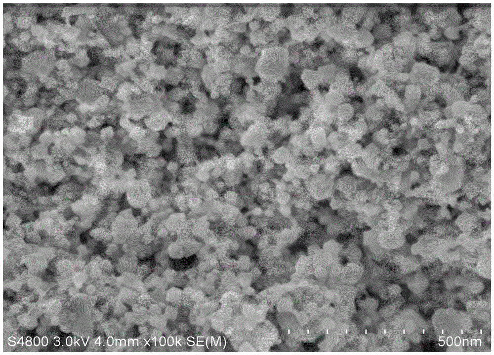
[0020] The GaN target with a purity of 99.99% and the copper foil are respectively placed in the sputtering chamber, the distance between the target and the substrate D=7cm; the cavity is evacuated to V≥1×10 -7 Torr and heat the substrate to 600°C; use magnetron sputtering to bombard the target to deposit and grow GaN on the metal substrate. Reactive gas N 2 Flow rate F=20sccm, working pressure P=100mTorr; sputtering power W=200w, deposition time 120mins. The prepared sample was characterized by SEM, figure 1 It can be seen that the sample is nanoparticles with an average size of about 40nm. The material obtained in Example 1 was made into a button battery according to the following method: the prepared GaN / Cu was cut into a disc with a diameter of 14 mm, and vacuum dried at 120° C. for 12 h. Lithium metal sheet is used as the counter electrode, Celgard membrane is used as the separator, and LiPF is dissolved 6 (1mol / L) EC+DEC (volume ratio 1:1) solution is the electrolyte, ass...
Embodiment 2
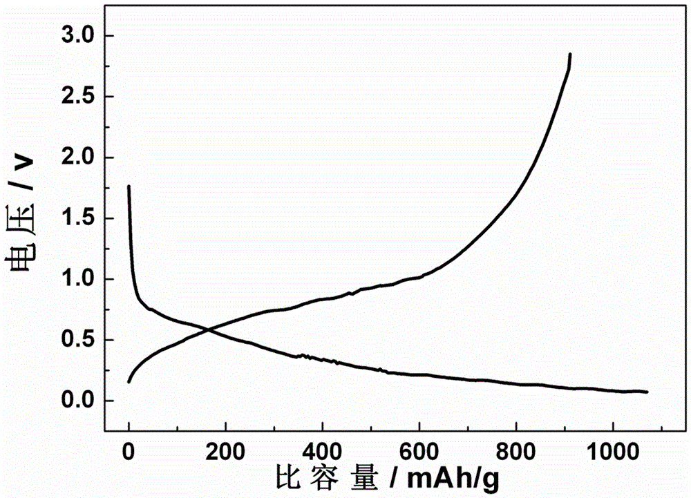
[0022] The GaN target with a purity of 99.99% and the foamed nickel are respectively placed in the sputtering chamber, the distance between the target and the substrate D=7cm; the chamber is evacuated to V≥1×10 -7 Torr and heat the substrate to 600°C; use magnetron sputtering to bombard the target to deposit and grow GaN on the metal substrate. Reactive gas N 2 Flow rate F=20sccm, working pressure P=100mTorr; sputtering power W=200w, deposition time 80mins. The material obtained in Example 2 was prepared into a button battery according to the steps in Example 1 and its electrochemical performance was studied. Such as image 3 As shown, the first charge and discharge capacities of the GaN prepared in Example 2 as the negative electrode of the lithium ion battery are 888 and 980 mAh / g, respectively.
Embodiment 3
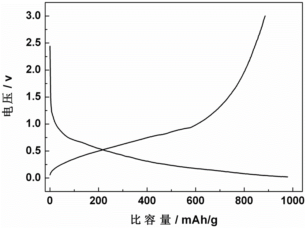
[0024] Place the GaN target with a purity of 99.99% and the foamed copper with pre-deposited graphene in the sputtering chamber. The distance between the target and the substrate is D=7cm; the chamber is evacuated to V≥1×10 -7 Torr and heat the substrate to 600°C; use magnetron sputtering to bombard the target to deposit and grow GaN on the metal substrate. Reactive gas N 2 Flow rate F=20sccm, working pressure P=100mTorr; sputtering power W=200w, deposition time 30mins. The material obtained in Example 2 was prepared into a button battery according to the steps in Example 1 and its electrochemical performance was studied. Such as image 3 As shown, the first charge and discharge capacities of the GaN prepared in Example 2 as the negative electrode of a lithium ion battery are 913 and 955 mAh / g, respectively.
PUM
 Abstract
Description
Claims
Application Information