Active layer, thin film transistor, array substrate, display device and manufacturing method

A thin-film transistor and active layer technology, applied in the direction of transistors, semiconductor/solid-state device manufacturing, semiconductor devices, etc., can solve problems such as the inability to form a bottom-gate staggered structure and the difficulty in controlling the thickness of the gate insulating layer, achieving controllable thickness, Effect of wide optical bandgap and high mobility

Active Publication Date: 2018-05-11
BOE TECH GRP CO LTD +1
View PDF4 Cites 0 Cited by
  • Summary
  • Abstract
  • Description
  • Claims
  • Application Information

AI Technical Summary

Problems solved by technology

The structure of the thin film transistor formed in this way will be very limited, for example, the bottom gate staggered structure cannot be formed, and it is difficult to control the thickness of the gate insulating layer

Method used


Image

  • Active layer, thin film transistor, array substrate, display device and manufacturing method
  • Active layer, thin film transistor, array substrate, display device and manufacturing method
  • Active layer, thin film transistor, array substrate, display device and manufacturing method

Examples


preparation example Construction

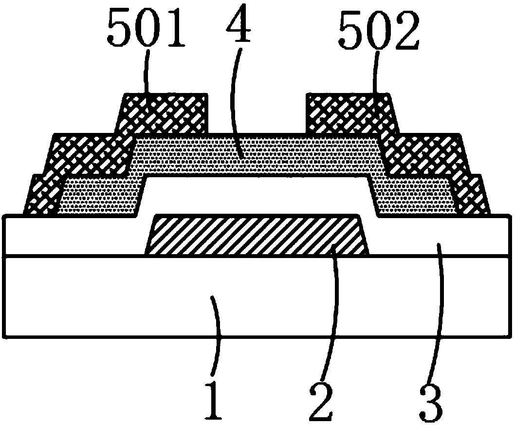
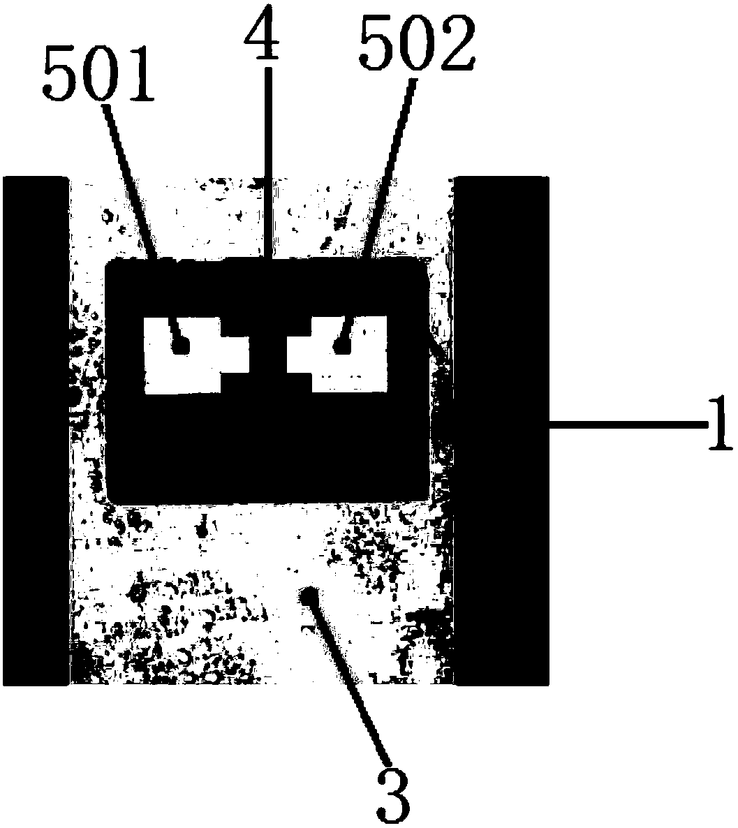
[0065] In the fifth aspect, an embodiment of the present invention provides a method for preparing an active layer. The method for preparing the active layer includes: preparing a zirconium indium oxide film with a preset thickness by DC sputtering, and then wet etching the pattern to obtain the active layer; wherein, as shown above, the chemical formula of zirconia indium is Zr x In 100-x o y , where 0.1≤x≤20, y>0.

[0066] It can be seen that the preparation method of the active layer provided by the embodiment of the present invention has the advantages of high film formation rate and simple process, and does not need to set a barrier layer on the active layer, which reduces the preparation cost.

[0067] Further, after wet etching the zirconia indium film, anneal the zirconia indium film at a temperature of 150-220° C. for at least 30 minutes in phosphoric acid with a mass concentration of 40%-60% to form the desired active layer. It can be seen that after the active l...

Embodiment 1

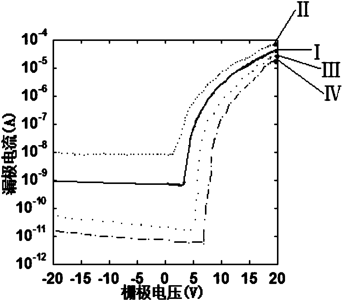
[0078] This embodiment provides an active layer, the thickness of which is 20nm, the material is zirconium oxide indium, and the chemical formula is Zr 1 In 91 o 100 , the carrier concentration is 1.5×10 18 cm -3 , with a carrier mobility of 31 cm 2 / Vs. Before the annealing, the etching rate of the active layer in the phosphoric acid of 50% mass concentration is equal to 60nm / min; The rate was 5 nm / min.

Embodiment 2

[0080] This embodiment provides an active layer with a thickness of 25nm, the material is zirconium oxide indium, and the chemical formula is Zr 6 In 94 o 100 , the carrier concentration is 1×10 18 cm -3 , with a carrier mobility of 30 cm 2 / Vs. Before the annealing, the etching rate of the active layer in the phosphoric acid of 50% mass concentration was equal to 65nm / min. The rate was 4nm / min.


PUM

PropertyMeasurementUnit
etching rateaaaaaaaaaa
carrier concentrationaaaaaaaaaa

Abstract

The invention discloses an active layer, a thin film transistor, an array substrate, a display device and a preparation method, and belongs to the field of flat panel displays. The material of the active layer is zirconia indium, and the chemical formula of zirconia indium is ZrxIn100‑xOy, where 0.1≤x≤20, y>0. Utilizing the active layer provided by the present invention, various structure types can be prepared by full DC sputtering, such as thin-film transistors with a bottom-gate staggered structure, and the obtained thin-film transistors have high carrier mobility and high electrical uniformity , and can ensure that the thickness of the gate insulating layer is controllable.

Description

technical field [0001] The invention relates to the field of flat panel display, in particular to an active layer, a thin film transistor, an array substrate, a display device and a preparation method. Background technique [0002] In the field of flat panel display, especially in the field of organic electroluminescent display, thin film transistor (ThinFilm Transistor, TFT for short), which is the core of its industry, has received more and more attention. At present, thin film transistors mainly include: a substrate, a gate, a gate insulating layer, an active layer, a source electrode and a drain electrode, wherein the source electrode and the drain electrode cover the active layer to form a back channel on the active layer structure, thereby realizing the small size and small parasitic capacitance of the thin film transistor. At present, the commonly used materials for the back channel structure in thin film transistors include silicon materials, oxide semiconductor mat...

Claims


Application Information

Patent Timeline
Patent Type & Authority Patents(China)
IPC IPC(8): H01L29/24H01L29/786H01L21/02H01L21/477H01L21/34
CPCH01L21/02565H01L21/02631H01L21/02667H01L21/477H01L29/24H01L29/66969H01L29/7869H01L21/30604H01L21/324H01L29/78618H01L21/34H01L27/1225H01L29/4908H01L29/66765H01L29/78603
Inventor 闫梁臣袁广才徐晓光王磊彭俊彪兰林锋
Owner BOE TECH GRP CO LTD
Why Eureka
Try Eureka