
A method of assembling nanoelectronic devices

A kind of electronic device and nanotechnology, applied in the direction of nanotechnology, nanotechnology, nanotechnology for materials and surface science, etc., can solve the problem that the interconnection manufacturing process of integrated circuits is no longer compatible, and achieve the effect of solving chaos and disorder

Active Publication Date: 2017-07-07
徐州鹏宇液压科技有限公司
View PDF7 Cites 0 Cited by
  • Summary
  • Abstract
  • Description
  • Claims
  • Application Information

AI Technical Summary

Problems solved by technology

However, since the scale of nanomaterials is on the nanometer scale, it is no longer compatible with the conventional integrated circuit interconnection manufacturing process. Therefore, how to realize the precise assembly of nanomaterials, so that the nanomaterials can be controllably assembled to the target structure according to the predetermined direction and density, And to form a firm and reliable low-resistance contact between assembled nanomaterials and metal electrodes has become a key issue in the application of nanomaterial interconnection.

Method used


Image

  • A method of assembling nanoelectronic devices
  • A method of assembling nanoelectronic devices
  • A method of assembling nanoelectronic devices

Examples


Embodiment 1

[0020] Step 1: If figure 1 As shown, the circuit system for assembling nanoelectronic devices is built, including high and low frequency AC power supply 1, adder 2, electric key 3, microelectrode pair 4, low-pass filter circuit 5, I / V conversion circuit 6, A / D conversion Circuit 7, lock-in amplifier 8, computer 9, wherein the spacing of microelectrodes is determined as 2 microns according to the size of zinc oxide zinc nanowires;

[0021] Step 2: drop the solution containing zinc oxide nanowires onto the pair of microelectrodes;

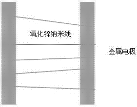
[0022] Step 3: Connect the circuit and output 10 6 The high frequency of HZ and the low frequency current of 50HZ, through the computer to observe the change of the electric signal of the circuit, control the closing of the electric key, and disconnect the electric key after five times of waveform changes, so that five zinc oxide nanowires are connected to the microelectrode pair, as in figure 2 shown;

[0023] Step 4: Use high-frequency ultrason...

Embodiment 2

[0025] Step 1: Build a circuit system for assembling nanoelectronic devices, including high and low frequency AC power supply 1, adder 2, electric key 3, microelectrode pair 4, low-pass filter circuit 5, I / V conversion circuit 6, A / D conversion Circuit 7, lock-in amplifier 8, computer 9, wherein the spacing of the microelectrode pair is set as 1 micron;

[0026] Step 2: drop the solution containing tungsten oxide nanoparticles onto the pair of microelectrodes;

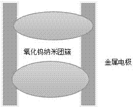
[0027] Step 3: Connect the circuit and output 10 5 HZ high-frequency and 30HZ low-frequency current, through the computer to observe the changes in the electrical signal of the circuit to control the closing of the electric key, and disconnect the electric key after two changes in the waveform, so that two zinc oxide nanoparticle clusters are overlapped on the microelectrode pair ,Such as image 3 shown;

[0028] Step 4: Use high-frequency ultrasonic energy to bond the assembled electronic devices.

Embodiment 3

[0030] Step 1: Build a circuit system for assembling nanoelectronic devices, including high and low frequency AC power supply 1, adder 2, electric key 3, microelectrode pair 4, low-pass filter circuit 5, I / V conversion circuit 6, A / D conversion Circuit 7, lock-in amplifier 8, computer 9, wherein the spacing of the microelectrode pairs is determined as 2 microns;

[0031] Step 2: drop the solution containing carbon nanotubes onto the pair of microelectrodes;

[0032] Step 3: Connect the circuit and output 10 7 The high frequency of HZ and the low frequency current of 50HZ, through the computer to observe the change of the electric signal of the circuit, control the closing of the electric key, and disconnect the electric key after the waveform changes, so that a single carbon nanotube is connected to the microelectrode pair;

[0033] Step 4: Use high-frequency ultrasonic energy to bond the assembled electronic devices.


PUM


Abstract

The invention provides a nano-electronic device mounting method. The nano-electronic device mounting method comprises the following steps: establishing a circuit system for mounting a nano-electronic device, wherein high-low-frequency current of a high-low-frequency alternating current power supply is connected with one end of a microelectrode pair through a switch after the high-low-frequency current is superposed by an adder, the other end of the microelectrode pair is connected with a filter circuit for filtering unused high-frequency wavebands, an I / V conversion circuit converts current signals into easy-to-detect voltage signals, an A / D conversion circuit performs A / D conversion circuit, a phase-locked amplifier recognizes required signals, and meanwhile, a computer is used for monitoring the signals and an intelligent and controllable mounting process is achieved through on and off control of the switch; mounting nano materials with the certain amount on the microelectrode pair; bonding a mounted electronic device by utilizing high-frequency ultrasonic energy. According to the nano-electronic device mounting method, the amount of the nano materials mounted on the electronic device is controllable, and the contact between the mounted nano materials and the microelectrode pair is reliable.

Description

technical field [0001] The invention relates to a method for assembling nanometer electronic devices, belonging to the technical field of nanometer materials. Background technique [0002] With people's demand for higher performance of integrated circuits, on the basis of ensuring the reliability of chips, the integration density of circuits integrated on chips continues to increase, and the width of interconnection lines continues to decrease. Aluminum interconnects prepared by the earliest etching method Connected to the current mainstream dual damascene copper interconnection technology, the manufacturing process continues to improve. However, the copper interconnection process is getting closer and closer to its critical limit due to problems such as electromigration failure, forcing the integrated circuit industry to seek new interconnection materials. Many nanomaterials are popular candidates for new interconnect materials because of their excellent electrical propert...

Claims


Application Information

Patent Timeline
Patent Type & Authority Patents(China)
IPC IPC(8): B81C3/00B82Y30/00B82Y40/00
CPCB81C3/001B81C2203/037B82Y30/00B82Y40/00
Inventor 赵波姜国华王楠
Owner 徐州鹏宇液压科技有限公司
Learn More