Semiconductor device manufacturing method and bonding assembly device

A manufacturing method and a technology for assembling devices, which are applied in semiconductor/solid-state device manufacturing, semiconductor devices, manufacturing tools, etc., can solve problems such as reduced heat dissipation characteristics, damage to semiconductor devices, and hindrance to heat dissipation, so as to reduce environmental loads, eliminate deviations, and prevent The effect of bad joint

Active Publication Date: 2018-10-23
FUJI ELECTRIC CO LTD
View PDF8 Cites 0 Cited by
  • Summary
  • Abstract
  • Description
  • Claims
  • Application Information

AI Technical Summary

Problems solved by technology

However, if there are air bubbles (voids) in the solder joint layer between the silicon wafer and the insulating substrate, or the solder joint layer between the insulating substrate and the metal base, these air bubbles hinder heat dissipation, thereby causing a significant decrease in heat dissipation characteristics. Causes damage to semiconductor devices

Method used


Image

  • Semiconductor device manufacturing method and bonding assembly device
  • Semiconductor device manufacturing method and bonding assembly device
  • Semiconductor device manufacturing method and bonding assembly device

Examples


Embodiment Construction

[0041] Hereinafter, embodiments of the present invention will be described with reference to the drawings. However, the present invention is not limited by the embodiments described below.

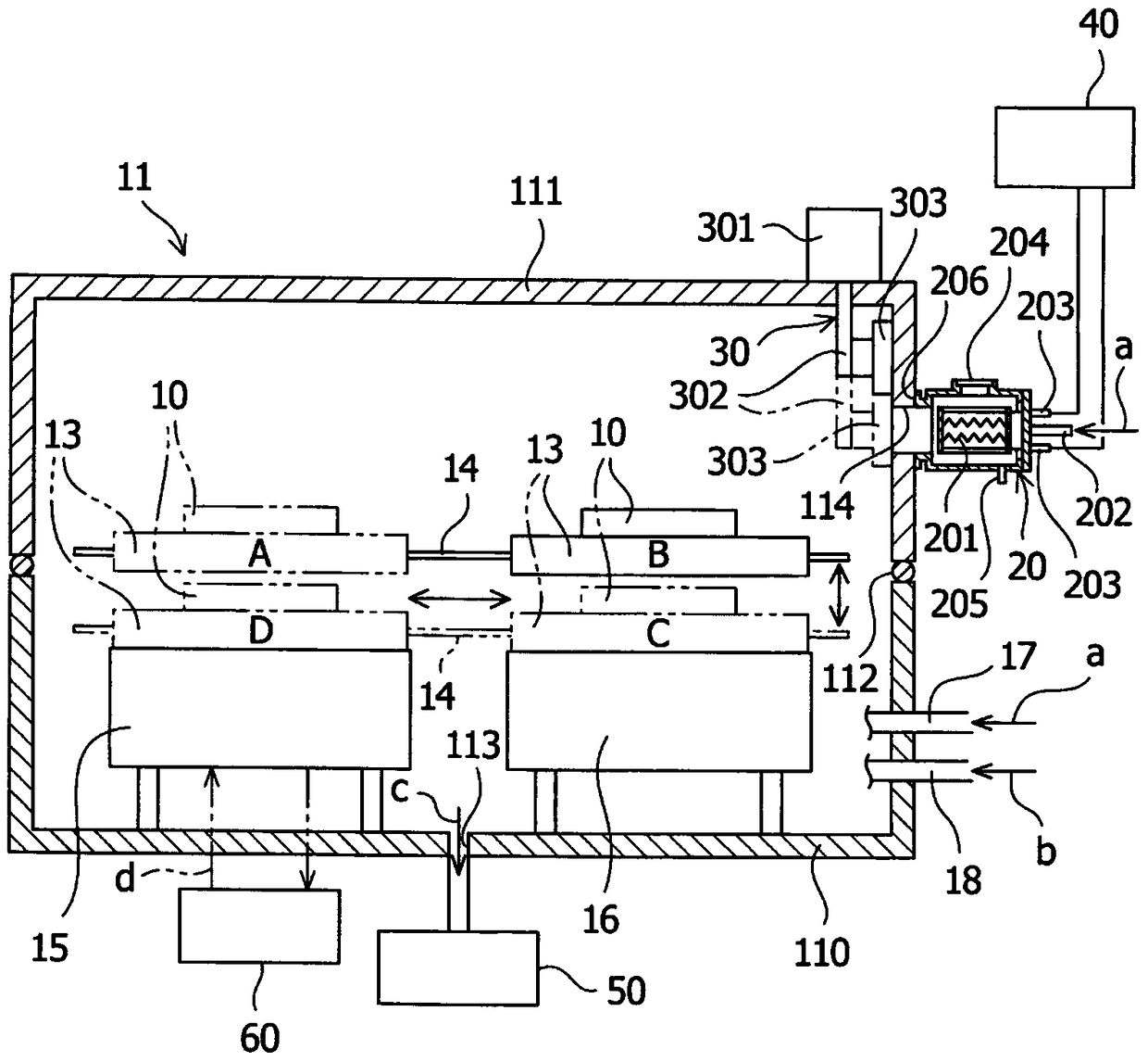
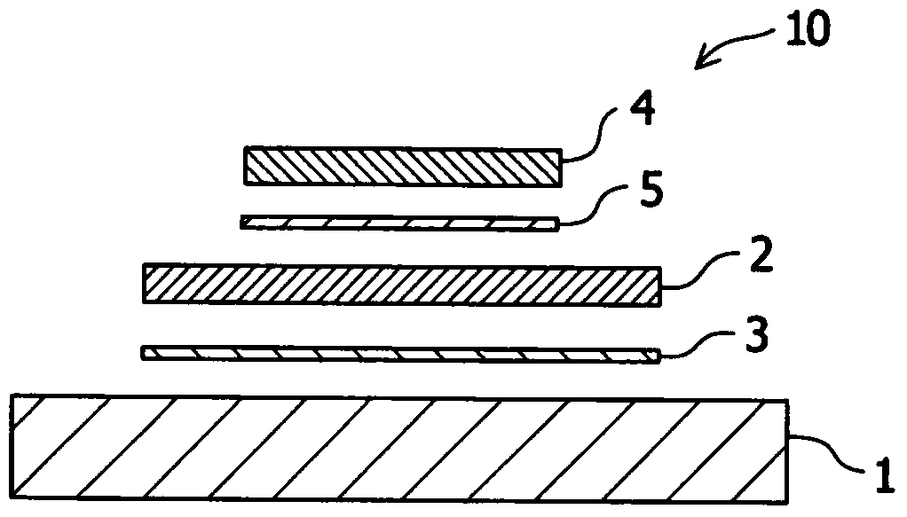
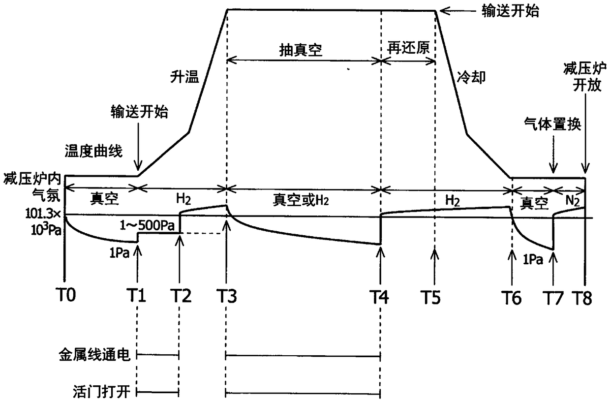
[0042] As a first embodiment of the present invention, a bonding and assembling apparatus suitably used in a method of manufacturing a semiconductor device including at least a heat ray heating step that can be opened and closed is described with reference to the drawings. The process of heating the metal wire outside the decompression furnace or in the decompression furnace with the partition wall.

[0043] figure 1 A schematic diagram of a joint assembly device according to an embodiment of the present invention is shown in . The bonding and assembling device mainly includes a conveying platform 13, a cooling plate 15, a hot plate 16, a reducing gas introduction pipe 17, and an inert gas introduction pipe 18 in the decompression furnace 11, and also has a The opening and closing part...


PUM

PropertyMeasurementUnit
melting pointaaaaaaaaaa

Abstract

A method of manufacturing a semiconductor device, comprising: a preparatory process of putting a laminated body including at least one member to be joined and a solder material into a decompression furnace; a decompression process of vacuum exhausting the decompression furnace; heat ray type In the heating process, the inside of the decompression furnace is set to a low-pressure hydrogen atmosphere, and the metal wire installed outside the decompression furnace with an openable and closable partition wall between the decompression furnace is heated, or the metal wire connected to the conveying table and the cooling plate is heated. And the metal wire installed in the decompression furnace through the partition wall that can be opened and closed between the hot plates is heated to generate atomic hydrogen; The next wall isolates the metal wire from the atmosphere in the decompression furnace; the heating step is to set the decompression furnace as a positive pressure hydrogen atmosphere and heat it to the bonding temperature to melt the solder material; and the bubble removal process is to maintain the bonding temperature In this state, the inside of the decompression furnace was set to a vacuum atmosphere again to remove air bubbles in the solder melt.

Description

technical field [0001] The present invention relates to a method of manufacturing a semiconductor device and a bonding assembly device used therefor. In particular, the present invention relates to a semiconductor device manufacturing method capable of manufacturing a semiconductor device having a higher-quality and more reliable solder joint layer than conventional ones, and a bonding assembly device used in the method and excellent in maintainability. Background technique [0002] Conventionally, the following three methods have been mainly practiced as methods for manufacturing power semiconductor devices. In the first method, first, a continuous furnace (tube furnace) with a reducing atmosphere is used to pre-dip tin (Japanese: 备备はんだ), and solder is placed on the back electrode of the silicon wafer. Next, the silicon wafer is soldered on the insulating substrate with this solder. After that, wire bonding is performed. Then, the member in which the silicon wafer is sol...

Claims


Application Information

Patent Timeline
Patent Type & Authority Patents(China)
IPC IPC(8): H01L21/60B23K1/00
CPCH01L24/32H01L24/75H01L24/83B23K1/0008B23K2101/40H01L2224/32145H01L2224/8319
Inventor 斋藤俊介渡边裕彦大西一永
Owner FUJI ELECTRIC CO LTD
Why Eureka
Try Eureka