Multilayer nanometer composite phase-transition thin film material and preparation method and application thereof

A nano-composite and thin-film material technology, applied in the field of microelectronic materials, can solve the problems of inability to meet information storage requirements, poor thermal stability of amorphous state, unfavorable storage density, etc., achieve excellent comprehensive phase change performance, and reduce heat loss , the effect of reducing the overall thermal conductivity

Active Publication Date: 2016-06-15
昆山模之特电子材料有限公司
View PDF5 Cites 12 Cited by
  • Summary
  • Abstract
  • Description
  • Claims
  • Application Information

AI Technical Summary

Problems solved by technology

[0003] In the prior art, among the factors affecting various performances of PCRAM, phase change materials are one of the decisive factors. At present, the research on phase change materials mainly focuses on the Ge-Sb-Te system, where Ge 2 Sb 2 Te 5 However, this material has some defects, such as the low crystallization temperature (about 160 ° C) makes the thermal stability of the amorphous state poor, and the high melting point (about 620 ° C) makes the crystal The energy required for the transition from the amorphous state to the amorphous state is relatively high, which is not conducive to the further improvement of storage density, and cannot meet the information storage requirements of the future high-speed and big data era.

Method used


Image

  • Multilayer nanometer composite phase-transition thin film material and preparation method and application thereof
  • Multilayer nanometer composite phase-transition thin film material and preparation method and application thereof
  • Multilayer nanometer composite phase-transition thin film material and preparation method and application thereof

Examples


Embodiment 1~6

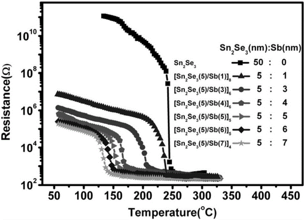
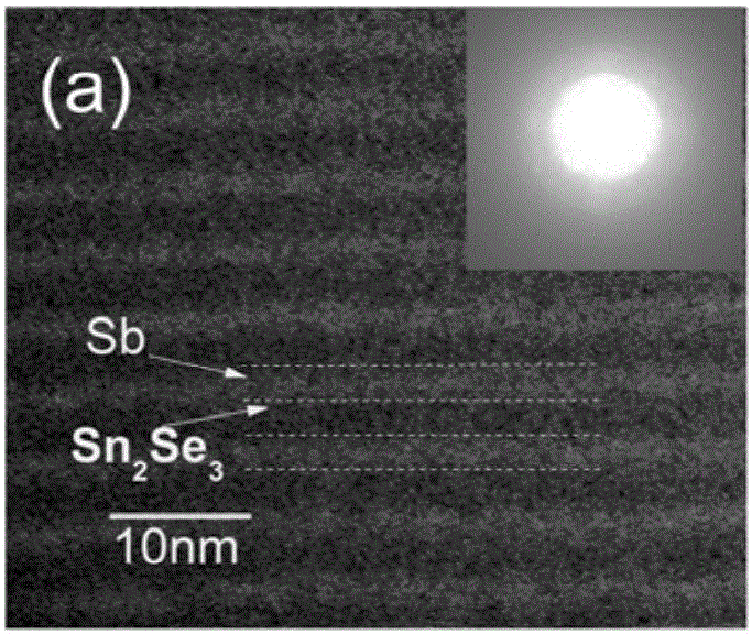
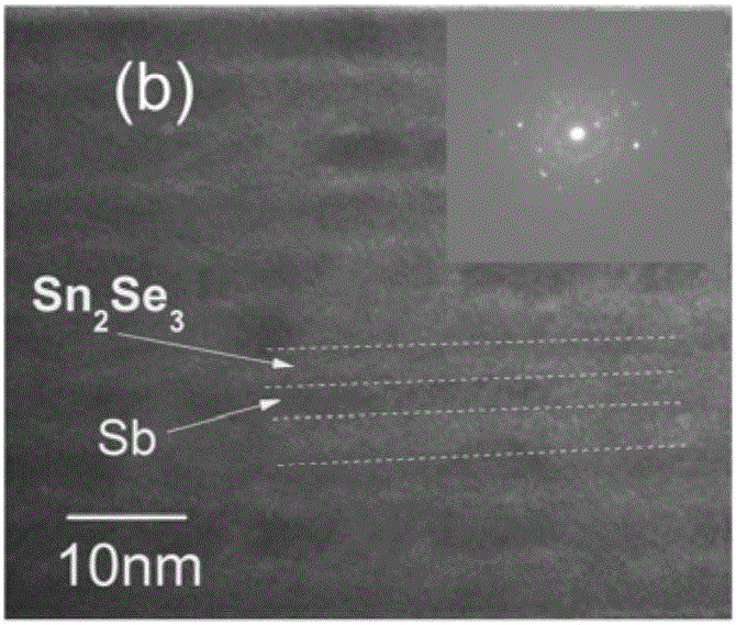
[0037] Examples 1-6 are respectively according to Sn 2 Se 3 / Sb multilayer nanocomposite phase change film with general structural formula [Sn 2 Se 3 (a) / Sb(b)] x Corresponding preparation [Sn 2 Se 3 (5nm) / Sb(1nm)] 8 , [Sn 2 Se 3 (5nm) / Sb(3nm)] 6 , [Sn 2 Se 3 (5nm) / Sb(4nm)] 6 , [Sn 2 Se 3 (5nm) / Sb(5nm)] 5 , [Sn 2 Se 3 (5nm) / Sb(6nm)] 5 , [Sn 2 Se 3 (5nm) / Sb(7nm)] 4 Six materials.

[0038] Above-mentioned six kinds of materials all make according to following preparation steps:

[0039] S1, cleaning SiO2 2 / Si(100) substrate, clean the surface and back, remove dust particles, organic and inorganic impurities, the specific cleaning steps are:

[0040] S10, wash with strong ultrasonic in acetone solution for 3-5 minutes, rinse with deionized water;

[0041] S11. Strong ultrasonic cleaning in ethanol solution for 3 to 5 minutes, rinse with deionized water, and use high-purity N 2 Blow dry the surface and back;

[0042] S12. Dry the water vapor in an oven a...


PUM

PropertyMeasurementUnit
thicknessaaaaaaaaaa
thicknessaaaaaaaaaa
thicknessaaaaaaaaaa

Abstract

The invention discloses a multilayer nanometer composite phase-transition thin film material and a preparation method and application thereof. The material is formed by arranging Sn2Se3 film layers and Sb film layers alternatively, one Sn2Se3 film layer and one Sb film layer serve as an alternative period, and the Sn2Se3 layer in the latter alternative period is deposited on the Sb layer in the former alternative period. A general formula of the film structure of the film material is [Sn2Se3(a)/Sb(b)]x, a represents the thickness of the single Sn2Se3 film layer, b represents the thickness of the single Sb film layer, a is greater than or equivalent to 1nm and lower than or equivalent to 50nm, b is greater than or equivalent to 1nm and lower than or equivalent to 50nm, x represents the number of alternative periods or layers of the Sn2Se3 film layers and Sb film layers, and x is a positive integer. The phase-transition thin film material uses Sb as a crystallization induction layer to accelerate phase transition of the phase-transition material, and advantages of low melting point and high thermal stability of Sn2Se3 are used; and the clamping effect of multiple interfaces in the multilayer nanometer composite structure is used to reduce the size of crystal grains, and further to shorten the crystallization time, inhibit crystallization, improve the thermal stability and accelerate phase transition.

Description

technical field [0001] The invention belongs to the technical field of microelectronic materials, and in particular relates to a multilayer nanocomposite phase-change thin film material and its preparation method and application. Background technique [0002] Phase change memory (PCRAM) is a non-volatile information memory with great application prospects. The main part of PCRAM is a phase change material based on chalcogenide compounds. The thermal effect of electric pulses is used to make the phase change material change reversibly between amorphous state (high resistance) and crystalline state (low resistance), so as to realize data synchronization. write and erase. [0003] In the prior art, among the factors affecting various performances of PCRAM, phase change materials are one of the decisive factors. At present, the research on phase change materials mainly focuses on the Ge-Sb-Te system, where Ge 2 Sb 2 Te 5 However, this material has some defects, such as the l...

Claims


Application Information

Patent Timeline
Patent Type & Authority Applications(China)
IPC IPC(8): H01L45/00C23C14/35C23C14/18C23C14/16C23C14/06
CPCC23C14/0623C23C14/165C23C14/185C23C14/352H10N70/881H10N70/231H10N70/8825H10N70/026
Inventor 吴冬燕章雯蒋爱如吴阳江
Owner 昆山模之特电子材料有限公司
Why Eureka
Try Eureka