Process for manufacturing efficient polycrystalline cell

A high-efficiency, battery technology, applied in sustainable manufacturing/processing, final product manufacturing, semiconductor/solid-state device manufacturing, etc., can solve problems such as difficulties, achieve good film density, good passivation effect, and easy to promote.

Inactive Publication Date: 2016-06-22
HEFEI & SOLAR TECH
View PDF6 Cites 5 Cited by
  • Summary
  • Abstract
  • Description
  • Claims
  • Application Information

AI Technical Summary

Problems solved by technology

Although these new technologies have greatly improved the efficiency of the entire crystalline silicon cell, for polycrystalline cells, polycrystalline RIE products or polycrystalline PERC products, it is difficult to achieve an industrialized cell efficiency of more than 19.5% or even 20%. more difficult

Method used


Image

  • Process for manufacturing efficient polycrystalline cell
  • Process for manufacturing efficient polycrystalline cell
  • Process for manufacturing efficient polycrystalline cell

Examples


Embodiment 1

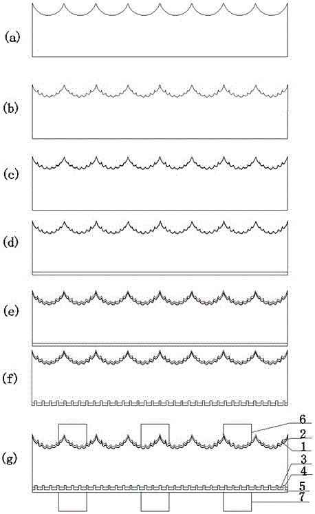
[0029] Such as Figure 2~3 As shown, in a preferred embodiment, the process for manufacturing high-efficiency polycrystalline cells of the present invention includes the following specific steps:

[0030] (1) Texturing: P-type polycrystalline silicon wafers are used to make texture according to the traditional polycrystalline wet method: that is, use Rena texturing machine, use a mixed solution of nitric acid and hydrofluoric acid with a mass ratio of 70:520, and make texture at a temperature of 6°C. Form the suede surface with light-trapping structure on the surface, and the silicon chip is corroded deeply about 2 microns in this step; image 3 as shown in (a);

[0031] (2) Reactive ion etching texturing : use the Tysol-RIE texturing machine produced by Changzhou Bitai Technology to carry out this step; use O 2 and SF 6 The reactive ions generated in the vacuum chamber of the texturing machine carry out bombardment etching on the surface of the silicon wafer, forming s...

Embodiment 2

[0042] In another preferred embodiment, the process for manufacturing high-efficiency polycrystalline cells of the present invention includes the following specific steps:

[0043] (1) Texturing: P-type polycrystalline silicon wafers are used to make texture according to the traditional polycrystalline wet method: that is, use a Schmid texture machine, use a mixed solution of nitric acid and hydrofluoric acid with a mass ratio of 70:520, and make texture at a temperature of 10°C. Form the suede surface with light-trapping structure on the surface, and the silicon wafer is corroded deeply about 5 microns in this step; image 3 as shown in (a);

[0044] (2) Reactive ion etching texturing : use the Tysol-RIE texturing machine produced by Changzhou Bitai Technology to carry out this step; use O 2 and SF 6 The reactive ions generated in the vacuum chamber of the texturing machine carry out bombardment etching on the surface of the silicon wafer, forming such as image 3 (b) ...

Embodiment 3

[0053] The process for manufacturing high-efficiency polycrystalline cells of the present invention comprises the following specific steps:

[0054] (1) Texturing: P-type polycrystalline silicon wafers are used to make texture according to the traditional polycrystalline wet method: that is, use Rena texturing machine, use a mixed solution of nitric acid and hydrofluoric acid with a mass ratio of 70:520, and make texture at a temperature of 8°C. Form the suede surface with light-trapping structure on the surface, and the silicon chip is corroded to a depth of about 4 microns in this step; image 3 as shown in (a);

[0055] (2) Reactive ion etching texturing : Use the Tysol-RIE texturing machine produced by Changzhou Bitai Technology to carry out this step; use SF 6 and Cl 2 The reactive ions generated in the vacuum chamber of the texturing machine carry out bombardment etching on the surface of the silicon wafer, forming such as image 3 (b) The shown nanoscale microstr...


PUM

PropertyMeasurementUnit
thicknessaaaaaaaaaa
thicknessaaaaaaaaaa
thicknessaaaaaaaaaa

Abstract

The invention discloses a process for manufacturing an efficient polycrystalline cell. The process includes the steps of silicon wafer surface texturing, diffusion, etching, silicon nitride thin film deposition, and printing and sintering in sequence, and is characterized in that a step of texturing through reactive ion etching is added between the silicon wafer surface texturing step and the diffusion step, a step of plating a Al2O3 film is added between the etching step and the silicon nitride thin film deposition step, the Al2O3 film is deposited on the reverse side of the silicon wafer, a laser grooving step is added between the silicon nitride thin film deposition step and the printing and sintering step, and laser grooving is performed on the Al2O3 film. The photoelectric conversion efficiency of a polycrystalline cell manufactured by application of the process provided by the invention can be improved.

Description

Technical field [0001] The invention involves the manufacturing process of photovoltaic batteries, which specifically involves a process of manufacturing high -efficiency polycrystalline batteries. Background technique [0002] The photovoltaic industry is in a period of rising development in the industry. After the rapids of technological innovation in recent years, it has gradually become close to the bottleneck, and the development of battery technology is essential to the entire photovoltaic industry.Traditional polycrystalline battery production process such as figure 1 Show, in six steps, in turn: (1) the surface of the silicon wafer; (2) diffusion; (3) etching; (4) silica nitride film deposition (PECVD); (5) printing sintering; (((5) sintering;6) Packaging.Among them, the surface of the silicon wafer surface is made of velvet according to the traditional polycrystal wet method. Even if nitric acid and hydrofluoric acid are mixed with a solution, the velvet is made at 6 ~ 1...

Claims


Application Information

Patent Timeline
Patent Type & Authority Applications(China)
IPC IPC(8): H01L31/18H01L31/0216H01L21/3065H01L21/316H01L21/3105
CPCH01L21/02178H01L21/0228H01L21/3065H01L21/3105H01L31/02167H01L31/02168H01L31/1804Y02E10/547Y02P70/50
Inventor 李奎朱生宾李陶谢伟崔廷蒋明强王凌祥
Owner HEFEI & SOLAR TECH
Why Eureka
Try Eureka