Preparation method and application of nano-semiconductor photocatalyst
A nano-semiconductor, photocatalyst technology, applied in chemical instruments and methods, physical/chemical process catalysts, nanotechnology, etc., can solve the problems of reducing the surface quality of silicon wafers, unstable oxidants, ion contamination, etc., and achieve high polishing removal rate. , No pits and bumps, less scratches
- Summary
- Abstract
- Description
- Claims
- Application Information
AI Technical Summary
Problems solved by technology
Method used
Image
Examples
Embodiment 1
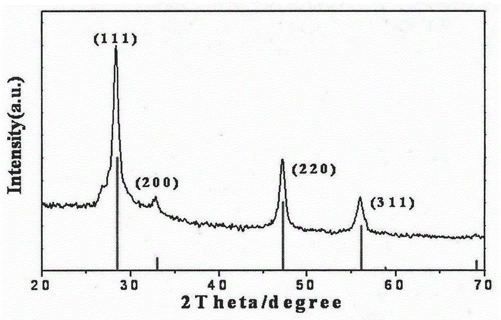
[0037] Under the protection of argon, put 6mmol elemental sulfur and 6ml oleylamine in a three-necked flask and stir at 120°C for 8h to form a dark red liquid. After cooling down to room temperature, pour it into a conical flask and store it in an oven at 50°C. The resulting dark red liquid is the sulfur precursor.
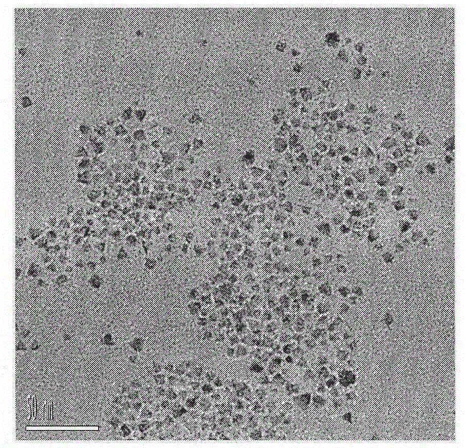
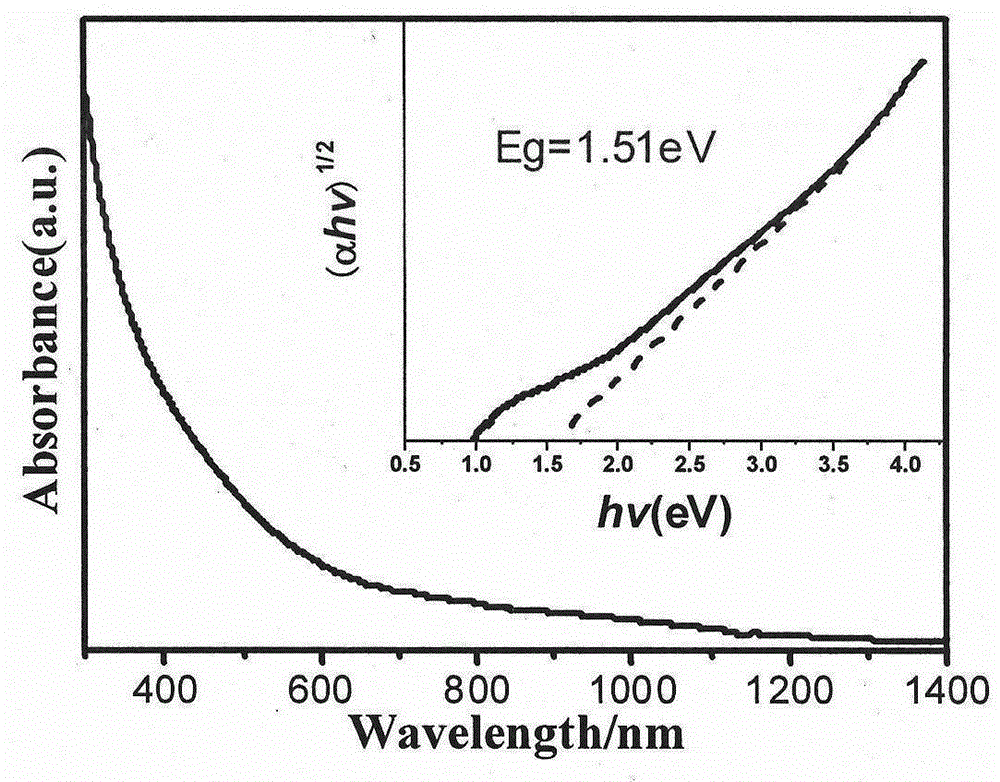
[0038] Weigh 1mmol of cuprous chloride, 0.5mmol of manganese chloride and 0.5mmol of tin tetroxide and add them to a three-necked bottle containing 50ml of oleylamine, stir and heat up to 120°C to vacuumize the three-necked bottle, and then add Introduce nitrogen, heat to 240°C (during this process, the metal salt slowly dissolves, and oleylamine changes from colorless to light yellow), inject the above-mentioned sulfur precursor quickly with an injection needle, and a black precipitate is generated immediately. After reacting for 1 h, the heating mantle was removed and cooled to room temperature. The resulting black precipitate was nano-Cu 2 MnSnS 4 nano-semico...
Embodiment 2
[0040]Under the protection of argon, put 4mmol elemental sulfur and 4ml oleylamine in a three-necked flask and stir at 120°C for 8h to form a dark red liquid. After cooling down to room temperature, pour it into a conical flask and store it in an oven at 50°C. The resulting dark red liquid is the sulfur precursor.
[0041] Weigh 2mmol of copper stearate, 1mmol of manganese stearate and 1mmol of tin stearate respectively and add them to a three-necked bottle containing 100ml of oleic acid. Stir and heat up to 120°C to evacuate the three-necked bottle, and then fill the three-necked bottle with Introduce nitrogen, heat to 270°C, quickly inject the above-mentioned sulfur precursor with an injection needle, and immediately produce a black precipitate. After reacting at this temperature for 1 hour, remove the heating mantle and cool to room temperature. The obtained black precipitate is nano-Cu 2 MnSnS 4 nano-semiconductor photocatalysts.
Embodiment 3
[0043] Under the protection of argon, put 2mmol thiourea and 4.0ml oleylamine in a conical flask, stir it on a heating plate at 180°C for 12h to form a light yellow liquid, after cooling down to room temperature, pour it into the conical flask and place it at 50°C Stored in an oven, the resulting light yellow liquid is the precursor of thiourea.
[0044] Weigh 0.5mmol copper chloride, 0.25mmol ferric chloride and 0.25mmol tin tetrachloride respectively and add them to a three-necked bottle containing 15ml of oleylamine, stir and heat up to 120°C to vacuumize the three-necked bottle, and then to three-necked Nitrogen was introduced into the neck bottle, heated to 250°C, and the above-mentioned thiourea precursor was quickly injected with an injection needle, and the reactant immediately changed from khaki to black precipitate. After reacting at this temperature for 1 hour, the heating mantle was removed and cooled to room temperature to obtain The black precipitate is nano Cu ...
PUM
| Property | Measurement | Unit |
|---|---|---|
| Mohs hardness | aaaaa | aaaaa |
Abstract
Description
Claims
Application Information
 - R&D
- Intellectual Property
- Life Sciences
- Materials
- Tech Scout
- Unparalleled Data Quality
- Higher Quality Content
- 60% Fewer Hallucinations
Browse by: Latest US Patents, China's latest patents, Technical Efficacy Thesaurus, Application Domain, Technology Topic, Popular Technical Reports.
© 2025 PatSnap. All rights reserved.Legal|Privacy policy|Modern Slavery Act Transparency Statement|Sitemap|About US| Contact US: help@patsnap.com


