Method to improve sonos memory read operation capability

A technology for reading operation and memory, which is applied in the field of improving SONOS memory reading operation ability, can solve problems such as adverse effects of SONOS transistor and transmission transistor current, adverse effects of circuit reading operation, and decline in reading operation ability, so as to improve reading Operation capability, good protection, effect of increasing read current

Active Publication Date: 2018-08-21
SHANGHAI HUAHONG GRACE SEMICON MFG CORP
View PDF7 Cites 0 Cited by
  • Summary
  • Abstract
  • Description
  • Claims
  • Application Information

AI Technical Summary

Problems solved by technology

[0004] The SONOS transistor is used to store and store the working state, that is, 0 or 1, and the transfer transistor is responsible for transmitting the stored working state; when the structure of the SONOS transistor shrinks, the gap D1 between the SONOS transistor and the transfer transistor gradually decreases, forming a gate After the sidewall, the gap D1 between the SONOS transistor and the transfer transistor is further reduced, for example, to 0.15 microns, and a layer needs to be grown before the source-drain injection Silicon dioxide 108 on the left and right, so that the gap between the SONOS transistor and the transfer transistor is filled with silicon dioxide 108, so that the gap between the SONOS transistor and the transfer transistor is due to two Blocked by the filling of silicon oxide 108, only a small amount of source and drain ions are implanted into the silicon substrate 101, that is, the junction depth and doping concentration of the finally formed source and drain regions 109c will be smaller than those of the source and drain regions 109a and 109b, which will Detrimentally affects the current flow of the SONOS transistor and the pass transistor, thereby adversely affecting the read operation of the circuit
Therefore, as the size of the cell structure of the SONOS memory continues to decrease, the read current of the SONOS memory formed by the existing method will decrease, and the read operation capability will decrease.

Method used


Image

  • Method to improve sonos memory read operation capability
  • Method to improve sonos memory read operation capability
  • Method to improve sonos memory read operation capability

Examples


Embodiment Construction

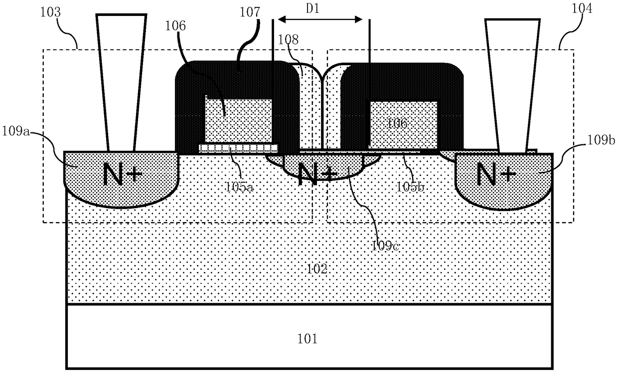
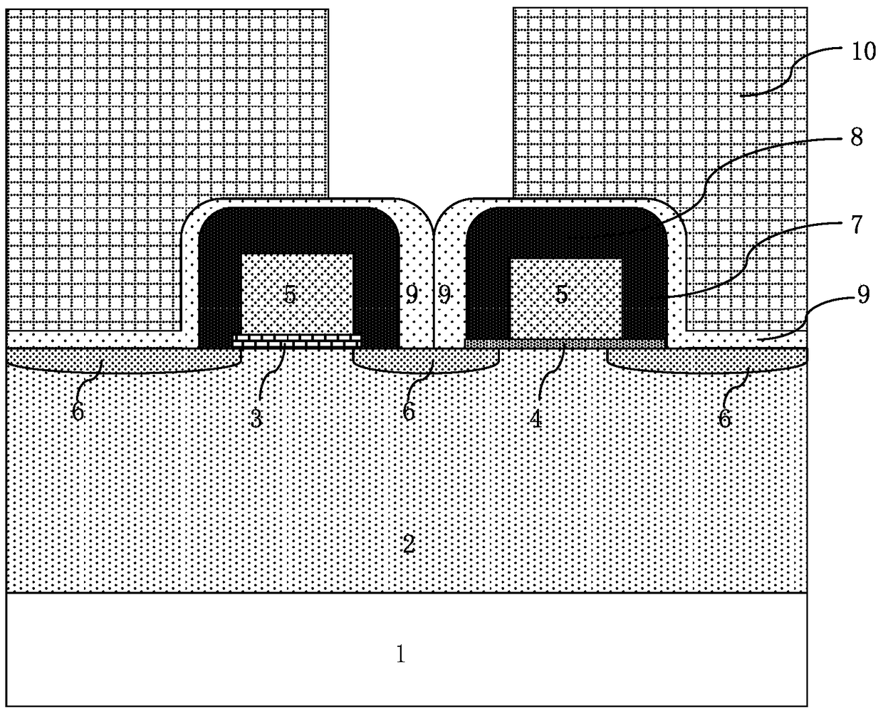
[0032] Such as figure 2 Shown is the flow chart of the method of the embodiment of the present invention; Figure 3A to Figure 3B Shown is a schematic diagram of the SONOS memory cell structure in each step of the method of the embodiment of the present invention. The cell structure of the SONOS memory of the method for improving the read operation capability of the SONOS memory in the embodiment of the present invention is composed of a SONOS transistor and an N-type transfer transistor, and the following steps are used to manufacture the cell structure of the SONOS memory:

[0033] Step 1, such as Figure 3A As shown, at first, forming the gate of the SONOS transistor and the N-type transfer transistor includes steps:

[0034] Step 11, forming a P well 2 on the silicon substrate 1, performing a turn-on voltage ion implantation in the P well 2 of the SONOS transistor region, and the formed turn-on ion implantation region is used to adjust the turn-on voltage of the SONOS tra...


PUM


Abstract

The invention discloses a method for improving SONOS memory reading operation capability. The method comprises steps that N-type light doping drain injection is carried out after formation of a grid electrode; a silicon nitride side wall is formed; a silicon dioxide layer for source and drain injection protection is formed at a front face of a silicon substrate; an NPC-level light cover is employed to from a first photoresist graph to define contact hole opening zones between grid electrodes of an SONOS transistor and an N-type transistor; the first photoresist graph is utilized as a mask layer for respectively etching the silicon dioxide layer and the silicon nitride side wall; source and drain injection is carried out. Through the method, the reading current of devices can be improved, and reading operation capability of the devices is improved.

Description

technical field [0001] The invention relates to a semiconductor integrated circuit manufacturing method, in particular to a method for improving the reading operation capability of SONOS memory. Background technique [0002] SONOS (Silicon-Silicon Oxide-Silicon Nitride-Silicon Oxide-Silicon) flash memory device has become one of the main flash memory device types at present because of its good scaling characteristics and radiation resistance characteristics. [0003] The cell structure of the existing SONOS memory consists of a SONOS transistor and a transfer transistor, such as figure 1 As shown, it is a schematic diagram of the structure of the existing SONOS memory cell; the area shown by the dotted line 103 is a SONOS transistor, the area shown by the dotted line 104 is a transfer transistor, and a P well 102 is formed on the surface of the silicon substrate 101, and the gate of the SONOS transistor The structure is composed of stacked ONO layer 105a and polysilicon gat...

Claims


Application Information

Patent Timeline
Patent Type & Authority Patents(China)
IPC IPC(8): H01L27/115H01L27/1157
Inventor 郭振强罗啸
Owner SHANGHAI HUAHONG GRACE SEMICON MFG CORP
Why Eureka
Try Eureka