Perpendicular LED chip structure and preparation method therefor

A LED chip and growth substrate technology, which is applied in semiconductor/solid-state device manufacturing, electrical components, circuits, etc., can solve the problems of poor structure and performance of GaN epitaxial layer, huge laser lift-off system, cracking of conductive substrate, etc., to achieve guaranteed Integrity and uniformity, increase spot overlap rate, and reduce the effect of substrate deformation

Active Publication Date: 2016-07-06
ENRAYTEK OPTOELECTRONICS
View PDF4 Cites 7 Cited by
  • Summary
  • Abstract
  • Description
  • Claims
  • Application Information

AI Technical Summary

Problems solved by technology

[0007] For the vertical process of wafers with a size of 4 inches or larger, the stress accumulated per unit area in the wafer increases greatly after bonding. If the stress is not released uniformly during the peeling process, it is easy to cause the bonded conductive substrate to crack or The deformation is serious, and it has a bad microscopic impact on the structure and performance of the GaN epitaxial layer, which directly leads to serious leakage, resulting in extremely low yield
This is also a technical problem that the current vertical structure LED wafer size is concentrated in 2inch and difficult to break through to 4inch.
[0008] Moreover, this problem cannot be solved simply by reducing the laser spot. When the laser spot is irradiated on the GaN at the interface through a transparent sapphire substrate, it is necessary to achieve a good connection between the laser spot and the spot to avoid damage caused by the overlap of the spot. The GaN layer is ruptured due to repeated irradiation at a certain place, which requires very strict accuracy of the scanning control system. At the same time, it is necessary to perform beam shaping on the spot under the premise of ensuring a high laser optical power density. This not only High requirements are placed on the laser output power, which increases the complexity of the laser optical system, which will result in a large and expensive laser lift-off system

Method used


Image

  • Perpendicular LED chip structure and preparation method therefor
  • Perpendicular LED chip structure and preparation method therefor
  • Perpendicular LED chip structure and preparation method therefor

Examples


Embodiment 1

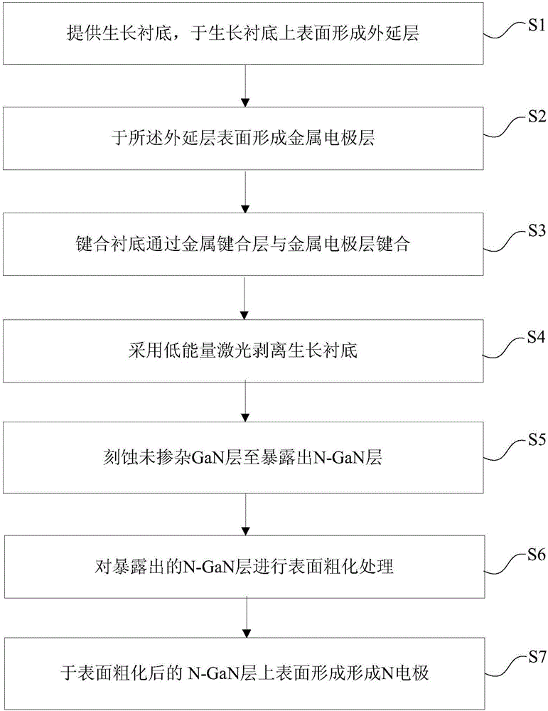
[0045] see Figure 1 to Figure 9 , the invention provides a method for manufacturing a vertical LED chip structure, the method for manufacturing a vertical LED chip structure at least includes the following steps:

[0046]S1: providing a growth substrate 101, and forming an epitaxial layer on the upper surface of the growth substrate 101;

[0047] S2: forming a metal electrode layer 106 on the surface of the epitaxial layer;

[0048] S3: the bonding substrate is bonded to the metal electrode layer 106 through the metal bonding layer;

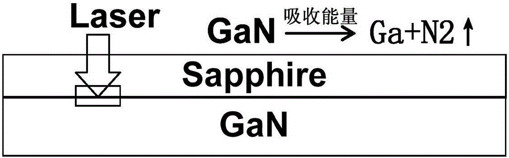
[0049] S4: Using a low-energy laser to lift off the growth substrate 101;

[0050] S5: etching the undoped GaN layer 102 to expose the N-GaN layer 103;

[0051] S6: performing surface roughening treatment on the exposed N-GaN layer 103;

[0052] S7: forming an N electrode 109 on the surface of the roughened N—GaN layer 103 .

[0053] In step S1, see figure 1 Step S1 in and Figure 4 , providing a growth substrate 101 , and forming an epi...

Embodiment 2

[0079] The present invention provides a vertical LED chip structure, please refer to Figure 9 , the vertical LED chip includes a bonded substrate and a P metal electrode layer 106, a P-GaN layer 105, a multi-quantum well layer 103, an N-GaN layer 103 and an N electrode formed sequentially on the bonded substrate from bottom to top 109.

[0080] Specifically, the growth substrate 101 may be a sapphire substrate, a silicon substrate, a silicon carbide substrate or a patterned substrate.

[0081] Specifically, the material of the metal bonding layer may be Au, Sn or AuSn alloy.

[0082] Specifically, the bonding substrate includes, but is not limited to, a Si sheet or a metal substrate with high electrical and thermal conductivity, such as a W / Cu substrate or a Mo / Cu substrate.

[0083] Specifically, the P metal electrode layer 106 includes a current spreading layer, a reflective layer and a metal bonding layer sequentially formed on the epitaxial layer. Wherein, the reflecti...


PUM

PropertyMeasurementUnit
diameteraaaaaaaaaa

Abstract

The invention provides a preparation method for a perpendicular LED chip structure. The preparation method comprises the steps of 1) providing a growth substrate, and forming an epitaxial layer on the growth substrate; 2) forming a metal electrode layer and a bonding substrate on the epitaxial layer in sequence; and 3) peeling off the growth substrate by low-energy laser, wherein the overlapping ratio of adjacent two small light spots is greater than 50%. The invention also provides the perpendicular LED chip structure, wherein the perpendicular LED chip structure comprises the bonding substrate, and the metal electrode layer, a P-GaN layer, a multi-quantum-well layer and an N-GaN layer which are positioned on the bonding substrate in sequence, and a passivation layer and an N electrode which are positioned on the surface of the N-GaN layer in sequence. By adoption of the preparation method, the problem of cracking or severe deformation of the bonding substrate easily caused by high wafer stress after bonding in the perpendicular process of the large-dimensional LED chip is solved; and meanwhile, the problems of severe electric leakage and extremely low rate of finished products directly caused by severe microcosmic influence of the epitaxial layer structure and the performance are also solved.

Description

technical field [0001] The invention belongs to the field of LED chips, in particular to a vertical LED chip structure and a preparation method thereof. Background technique [0002] As we all know, due to the constraints of non-conductivity and poor thermal conductivity of the sapphire substrate, the traditional front-mount LED chip has inherent defects such as uneven current distribution and poor heat dissipation. In order to overcome these shortcomings of the front-mount LED chip, the industry is actively developing a vertical-structure LED chip (hereinafter referred to as V-LED). V-LED adopts Si or metal substrate with high conductivity and good heat dissipation. The substrate has good heat conduction, the heat dissipation problem of PN junction is solved, and large-size power chips can be realized. [0003] The two electrodes of the V-LED chip are on both sides of the LED epitaxial layer. Since the patterned electrodes and all the P-type confinement layers are used as ...

Claims


Application Information

Patent Timeline
Patent Type & Authority Applications(China)
IPC IPC(8): H01L33/00H01L33/22H01L21/268H01L21/67
CPCH01L21/268H01L21/67103H01L33/0093H01L33/22
Inventor 吕孟岩徐慧文李起鸣
Owner ENRAYTEK OPTOELECTRONICS
Why Eureka
Try Eureka