Ultraviolet GaN-based LED epitaxy structure and manufacturing method thereof

An epitaxial structure and ultraviolet technology, applied in the direction of electrical components, circuits, semiconductor devices, etc., can solve the problems of reduced luminous efficiency, serious polarization electric field, severe energy band bending, etc., to weaken the energy band bending, increase the recombination probability, The effect of improving luminous efficiency

Inactive Publication Date: 2016-07-06
FOCUS LIGHTINGS SCI & TECH
View PDF5 Cites 6 Cited by
  • Summary
  • Abstract
  • Description
  • Claims
  • Application Information

AI Technical Summary

Problems solved by technology

However, an excessively high Al composition makes the polarization electric field more serious, and the energy band bends more severely, causing some electrons to escape to the p-layer through the quantum barrier, because these electrons are not effectively recombined with holes, resulting in a decrease in luminous efficiency

Method used


Image

  • Ultraviolet GaN-based LED epitaxy structure and manufacturing method thereof
  • Ultraviolet GaN-based LED epitaxy structure and manufacturing method thereof
  • Ultraviolet GaN-based LED epitaxy structure and manufacturing method thereof

Examples


Embodiment 1

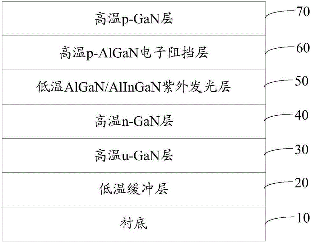
[0068] The ultraviolet GaN-based LED epitaxial structure in this embodiment includes from bottom to top:

[0069] The substrate is a patterned sapphire substrate or a flat sapphire substrate.

[0070] Low-temperature buffer layer (grown under the conditions of 540°C and 300 Torr), the low-temperature buffer layer is a low-temperature GaN layer with a thickness of 30nm.

[0071] High-temperature u-GaN layer (grown under the conditions of 1080°C and 200Torr), the thickness of this layer is 3um.

[0072] High-temperature n-GaN layer (grown under the conditions of 1060°C and 200Torr), the thickness of the layer is 3um, and the doping concentration is 8E18.

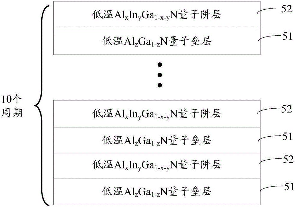
[0073] Low-temperature AlGaN / AlInGaN ultraviolet light-emitting layer (grown under the conditions of 800°C and 250 Torr), this layer is n-doped, and the doping concentration is 2E17. ginseng figure 2As shown, the low-temperature AlGaN / AlInGaN ultraviolet light-emitting layer includes 10 cycles of 5nm-thick low-temperature ...

Embodiment 2

[0087] The ultraviolet GaN-based LED epitaxial structure in this embodiment includes from bottom to top:

[0088] The substrate is a patterned sapphire substrate or a flat sapphire substrate.

[0089] Low-temperature buffer layer (grown under the conditions of 540°C and 300 Torr), the low-temperature buffer layer is a low-temperature GaN layer with a thickness of 30nm.

[0090] High-temperature u-GaN layer (grown under the conditions of 1080°C and 200Torr), the thickness of this layer is 3um.

[0091] High-temperature n-GaN layer (grown under the conditions of 1060°C and 200Torr), the thickness of the layer is 3um, and the doping concentration is 8E18.

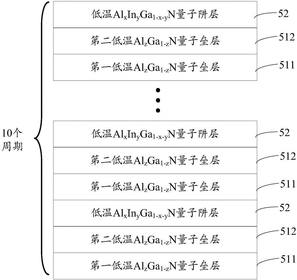
[0092] Low-temperature AlGaN / AlInGaN ultraviolet light-emitting layer (grown under the conditions of 800°C and 250 Torr), this layer is n-doped, and the doping concentration is 2E17. ginseng image 3 As shown, the low-temperature AlGaN / AlInGaN ultraviolet light-emitting layer includes 10 cycles of 5nm-thick low-temperature ...


PUM


Abstract

The invention provides an ultraviolet GaN-based LED epitaxy structure and a manufacturing method thereof. The LED epitaxy structure sequentially comprises a substrate, a low-temperature buffer layer, a high-temperature u-GaN layer, a high-temperature n-GaN layer, a low-temperature AlGaN / AlInGaN ultraviolet light-emitting layer, a high-temperature p-AlGaN electron blocking layer and a high-temperature p-GaN layer. By designing a quantum well light-emitting layer in the ultraviolet GaN-based LED epitaxy structure, the influences of spontaneous and piezoelectric polarization effects in the material are reduced; and the internal quantum efficiency of an ultraviolet LED device can be improved.

Description

technical field [0001] The invention relates to the technical field of LEDs, in particular to an ultraviolet GaN-based LED epitaxial structure and a manufacturing method thereof. Background technique [0002] A light-emitting diode (Light-EmittingDiode, LED) is a semiconductor electronic component that can emit light. This electronic component appeared as early as 1962. In the early days, it could only emit red light with low luminosity. Later, other monochromatic light versions were developed. Today, the light that can be emitted has covered visible light, infrared rays and ultraviolet rays, and the luminosity has also increased to a considerable extent. of luminosity. And the use is also used as indicator lights, display panels, etc. from the beginning; with the continuous advancement of technology, light-emitting diodes have been widely used in displays, TV lighting decoration and lighting. [0003] UV Light Emitting Diode (UV-LED) is a solid-state semiconductor device ...

Claims


Application Information

Patent Timeline
Patent Type & Authority Applications(China)
IPC IPC(8): H01L33/06H01L33/00
CPCH01L33/06H01L33/0075
Inventor 冯猛陈立人刘恒山
Owner FOCUS LIGHTINGS SCI & TECH
Why Eureka
Try Eureka