
High-temperature non-pressure seamless sintering technology-based miniaturized millimeter wave transmitting and receiving assembly

A technology of transmitting and receiving components and millimeter waves, which is applied in the directions of electrical components, transmission systems, magnetic field/electric field shielding, etc., can solve the problems of narrow communication frequency band, complex structure, and large amount of debugging, etc. secondary damage effect

Active Publication Date: 2016-07-06
NANJING CAIHUA TECH GROUP
View PDF3 Cites 3 Cited by
  • Summary
  • Abstract
  • Description
  • Claims
  • Application Information

AI Technical Summary

Problems solved by technology

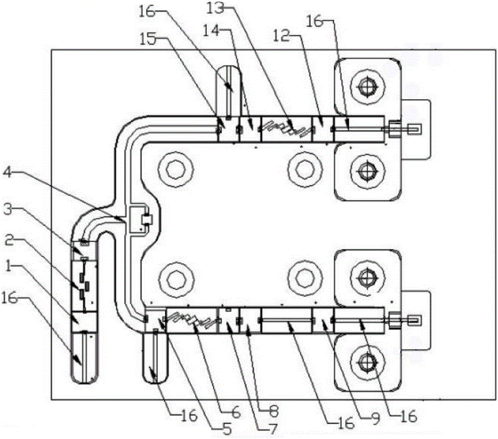
[0003] The purpose of the present invention is to provide a miniaturized millimeter-wave transceiver component based on high-temperature pressureless seamless sintering technology. By improving the structure and process, the existing millimeter-wave transceiver component has a complex structure, a large volume, a large amount of debugging, and low reliability. , narrow communication frequency band, and provide a miniaturized millimeter-wave transceiver component with excellent performance, which is compact in structure and easy to debug, and can effectively meet the requirements of ultra-wideband and high-speed millimeter-wave communication systems

Method used


Image

  • High-temperature non-pressure seamless sintering technology-based miniaturized millimeter wave transmitting and receiving assembly
  • High-temperature non-pressure seamless sintering technology-based miniaturized millimeter wave transmitting and receiving assembly
  • High-temperature non-pressure seamless sintering technology-based miniaturized millimeter wave transmitting and receiving assembly

Examples


Embodiment Construction

[0017] Below in conjunction with accompanying drawing and embodiment, content of the invention will be further described:

[0018] In the existing technology, this product uses more MMIC chips, and the MMIC chips are all made of 99.6% aluminum oxide substrate material. The expansion coefficient of the substrate material is 7.5. The shielding box selected by the existing millimeter wave transceiver components is basically For copper or aluminum alloy, the expansion coefficient of the profile is about 20, which is quite different from the expansion coefficient of the substrate material, so it is difficult to carry out high-temperature seamless sintering. At the same time, the MMICs of the existing millimeter-wave transceiver components are connected by a microstrip printed board. The microstrip printed board and the MMIC chip are pasted on the shielding box body through conductive silver paste. The conductive silver paste is unevenly coated, and the thickness of the MMIC chip ( ...


PUM


Abstract

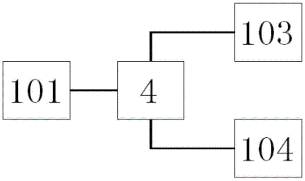
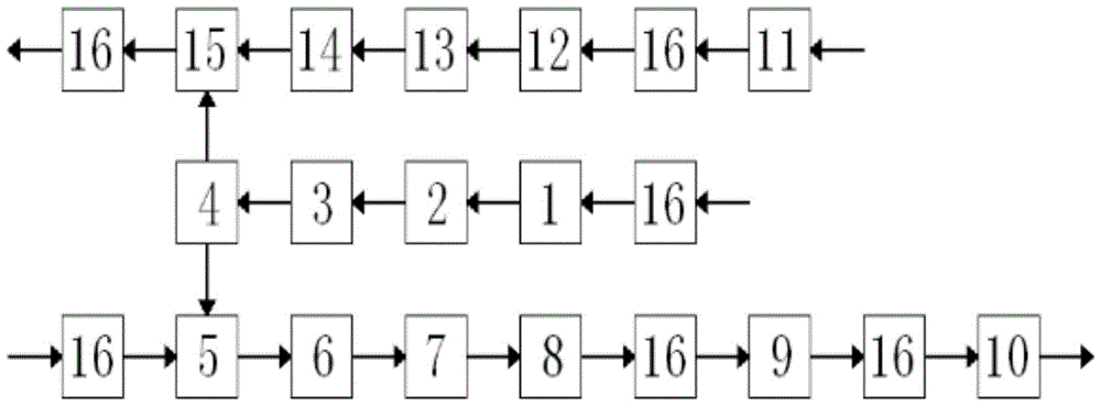
The invention discloses a high-temperature non-pressure seamless sintering technology-based miniaturized millimeter wave transmitting and receiving assembly. The high-temperature non-pressure seamless sintering technology-based miniaturized millimeter wave transmitting and receiving assembly includes a shielding box body, a local vibration frequency multiplication link, a power allocation link, a receiving link and a transmitting link; the local vibration frequency multiplication link is connected with the power allocation link; the power allocation link is connected with the receiving link and the transmitting link; a 85:15 tungsten copper alloy shielding box body is adopted as the shielding box body; the links are in direct bonded connection with adjacent MMIC chips through 25 um golden wires; conversion can be realized through glass insulator and copper bar high-temperature sintered integrated probe waveguides. The high-temperature non-pressure seamless sintering technology-based miniaturized millimeter wave transmitting and receiving assembly of the invention has the advantages of compact structure and easiness in debugging, and can effectively meet the requirements of an ultra-wide-band and high-speed millimeter wave communication system.

Description

technical field [0001] The invention belongs to the technical field of millimeter wave communication, and in particular relates to a miniaturized millimeter wave transceiver component based on high-temperature pressureless seamless sintering technology. Background technique [0002] The millimeter-wave wireless transceiver system mainly relies on the millimeter-wave transceiver component to convert high-frequency signals and intermediate-frequency signals, which is an important part of the millimeter-wave communication system. The existing millimeter-wave transceiver components all use conductive silver paste to paste the PCB printed board and MMIC chip on the aluminum shielding box. The MMIC chips are connected by the microstrip line on the PCB printed board, resulting in complex structure and bulky Huge, large amount of debugging, low reliability. At the same time, the waveguide coaxial conversion adopts the microstrip line transition, which is limited by the precision of...

Claims


Application Information

Patent Timeline
Patent Type & Authority Applications(China)
IPC IPC(8): H04B1/40H05K9/00
CPCH04B1/40H05K9/0026
Inventor 张君韩琳欧阳建伟杨广举康国新
Owner NANJING CAIHUA TECH GROUP
Learn More