Manufacturing method for semiconductor disease chip

A semiconductor and disease technology, which is applied in the manufacture of semiconductor disease chips and the surface functionalization of metal compounds, can solve problems such as weak signals and limited sensitivity of optical detectors

Inactive Publication Date: 2016-07-13
杭州格磊思沃科技有限公司
View PDF7 Cites 4 Cited by
  • Summary
  • Abstract
  • Description
  • Claims
  • Application Information

AI Technical Summary

Problems solved by technology

Due to the limited sensitivity of optical detectors, the general detection needs to amplify the fluorescent signal. For nucleic acid samples, it can be achieved by amplification. However, other complex biological macromolecules such as proteins and sugars cannot be simply amplified and cloned, so the signal is weak.

Method used


Image

  • Manufacturing method for semiconductor disease chip

Examples


Embodiment 1

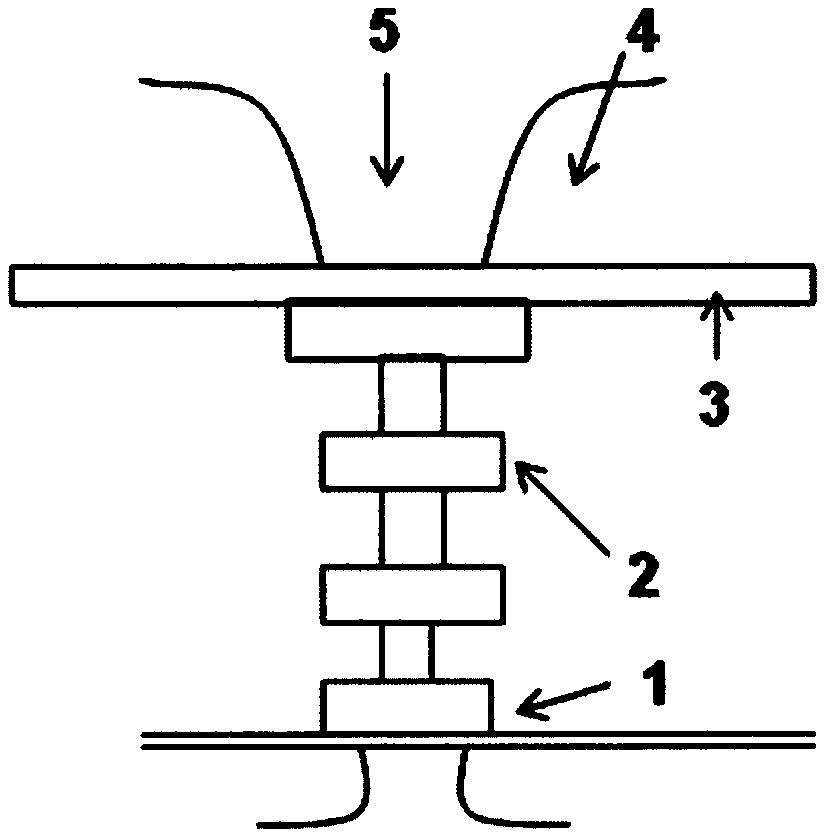
[0041] figure 1 Shown is a structural diagram of a semiconductor disease detection chip, including a metal oxide field effect transistor 1, one or more metal layers 2 connecting the gate of the metal oxide field effect transistor and the detection well, a metal compound layer 3 and an oxide layer 4 And detection well 5.

[0042]First, on the semiconductor wafer, a metal oxide field effect transistor as a sensor is fabricated, and one or more layers of metal are formed on the transistor to connect the gate of the transistor to the metal compound layer, and then an oxide layer is formed on the metal compound layer, And a detection well is formed, the detection well is square, and the side length is greater than 70 μm and less than 120 μm; the detection well can also be circular, and the diameter is greater than 70 μm and less than 120 μm. The metal compound layer is TaO 2 , the oxide film layer 2 is SiO 2 , the oxide thickness is 40 μm.

[0043] After the monoclonal HBeAb is...

Embodiment 2

[0046] Metal compound TaO 2 The method for surface functionalization mainly comprises the following steps:

[0047] 1. Prepare target solution: 15.0mg n-dodecyl diammonium phosphate (DDPO 4 (NH 4 ) 2 ) was dissolved in 5 mL of high-purity water, heated to 50°C, diluted with water to 100 mL, cooled to room temperature and filtered through a 0.22 μm filter to adjust the volume of the solution to 100 mL.

[0048] 2. Growth of monomolecular layer of dodecyl phosphate on the surface: Ultrasonic the chip in ultrapure water and 2-propanol for 15 minutes respectively, blow dry with nitrogen gas, transfer to oxygen plasma cleaning, and immediately transfer to glass vial after 3 minutes , join DDPO 4 (NH 4 ) 2 Solution, soaked for 48h, rinsed with 10mL ultrapure water, and dried with nitrogen.


PUM

PropertyMeasurementUnit
thicknessaaaaaaaaaa
thicknessaaaaaaaaaa
thicknessaaaaaaaaaa

Abstract

The invention relates to the field of bioelectronics and discloses an addressable semiconductor disease chip and a manufacturing method thereof. The semiconductor disease chip comprises a semiconductor chip and detection wells. The invention also relates to a surface functionalization method and a detection method. The semiconductor chip is characterized by comprising at least one sensor array and a detection well array above the sensors correspondingly, wherein the sensors are connected through a circuit; the positions of all the wells are confirmed and the wells are not interfered from each other.Detection indexes for specific diseases are fixed in the wells; target molecules enter into the detection wells and can have special reactions; corresponding enzymes can catalyze substrates for changing ion concentration; the sensors can sense the pH change in the detection wells so as to generate an electric signal. One well at most is corresponding to one index or one disease or a plurality of wells are corresponding to different indexes of one disease, and thus the multi-index simultaneous detection can be realized. The position of strong signal is corresponding to the well with active reaction, namely, to the to-be-detected index in the well.

Description

technical field [0001] The invention relates to the field of bioelectronics, in particular to a metal compound surface functionalization, a semiconductor disease chip, and a method for manufacturing the semiconductor disease chip. Background technique [0002] With the development of modern medical technology, doctors rely more and more on professional test results for accurate diagnosis of patients' diseases. Early detection of diseases in time and prescribing the right medicine will help improve the quality of life of patients and reduce the social medical and economic burden. [0003] There are many types of diseases, such as tuberculosis, hepatitis, bird flu, etc., and the corresponding antibody DNAs of different types and even origins of the same disease are different. Such as tuberculosis, the pathogenic bacteria that cause tuberculosis include Mycobacterium tuberculosis (M.tuberculosis), Mycobacterium bovis (M.bovis), Mycobacterium leprae (M.leprae), etc., and there a...

Claims


Application Information

Patent Timeline
Patent Type & Authority Applications(China)
IPC IPC(8): G01N27/414
CPCG01N27/4145
Inventor 谈忠琴戴丰加
Owner 杭州格磊思沃科技有限公司
Why Eureka
Try Eureka