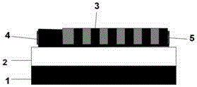
SOUP structured electrooptic modulator based on stark effect and manufacturing method
An optoelectronic modulator and Stark effect technology, applied in the field of electronics, can solve the problems affecting crystal epitaxial growth, complex high-voltage process conditions, affecting the optoelectronic performance of devices, etc. The effect of lattice mismatch
- Summary
- Abstract
- Description
- Claims
- Application Information
AI Technical Summary
Problems solved by technology
Method used
Image
Examples
Embodiment 1
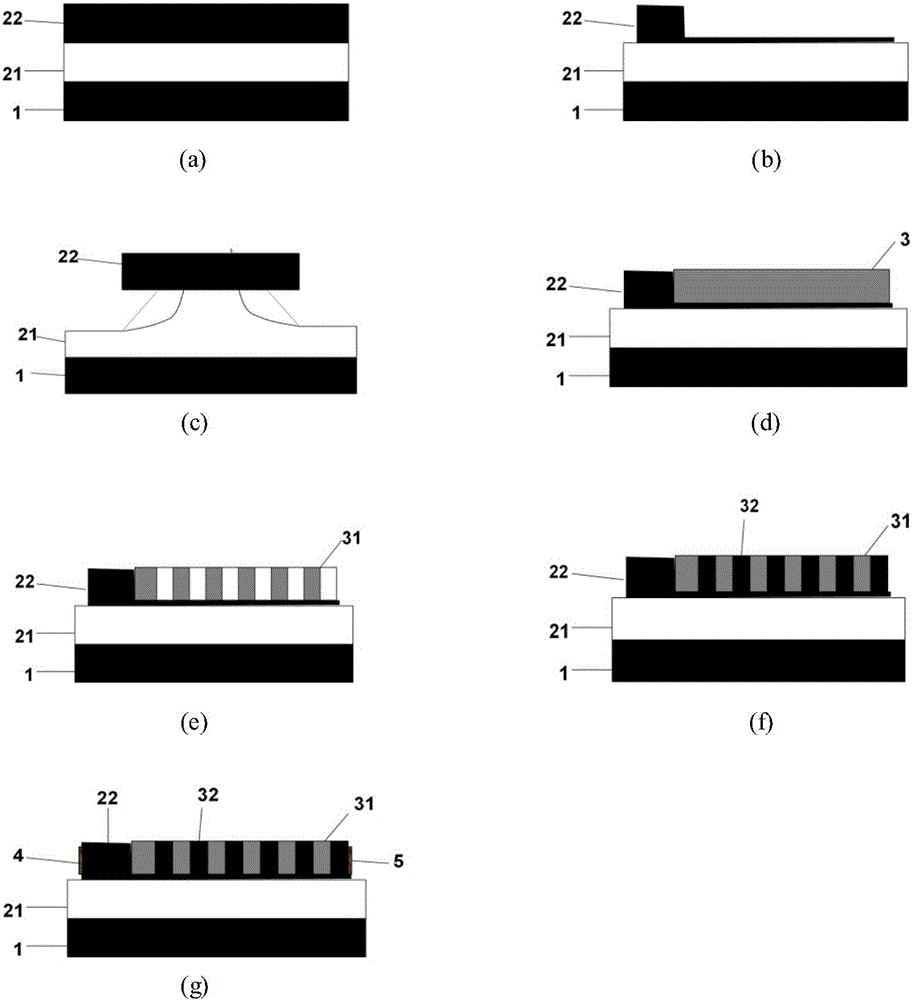
[0053] Embodiment 1: with Ge 2 h 6 As a precursor gas to prepare SOUP structure optoelectronic modulator based on Stark effect.
[0054] Step 1: Oxygen injection isolation.
[0055] Using the oxygen injection isolation method, the dose was 1.8×10 18 cm-2, oxygen ions with an energy of 200KeV are implanted into silicon to form a buried oxide layer SiO in silicon 2 , to get SiO located in the buried oxide layer 2 The structure of the waveguide above the silicon and the buried oxide layer SiO 2 The structure of the underlying silicon substrate, such as image 3 (a) shown.
[0056] Step 2: Etching the silicon waveguide.
[0057] Using the etching process, after etching the left and right ends of the silicon waveguide to remove one percent of the length of the silicon waveguide, thin the right side of the silicon waveguide to 7%-8% of the thickness before etching the silicon waveguide, and then use acetone and Plasma cleaning for 15 minutes, removing the photoresist, and ob...
Embodiment 2
[0068] Embodiment 2: with Si 2 h 6 As a precursor gas to prepare SOUP structure optoelectronic modulator based on Stark effect.
[0069] Step 1: Oxygen injection isolation.
[0070] Using the oxygen injection isolation method, the dose was 1.8×10 18 cm-2, oxygen ions with an energy of 200KeV are implanted into silicon to form a buried oxide layer SiO in silicon 2 , to get SiO located in the buried oxide layer 2 The structure of the waveguide above the silicon and the buried oxide layer SiO 2 The structure of the underlying silicon substrate, such as image 3 (a) shown.
[0071] Step 2: Etching the silicon waveguide.
[0072] Using the etching process, after etching the left and right ends of the silicon waveguide to remove one percent of the length of the silicon waveguide, thin the right side of the silicon waveguide to 7%-8% of the thickness before etching the silicon waveguide, and then use acetone and Plasma cleaning for 15 minutes, removing the photoresist, and ob...
PUM
 Abstract
Description
Claims
Application Information


