Coupler structure based on BCB bonding technology and production method thereof

A technology of coupling structure and bonding process, which is applied in the field of integrated optoelectronics, can solve the problems of inconvenient production, large size of coupling structure, and difficult coupling efficiency, etc., and achieve the effects of reducing production cost, stable coupling efficiency, and reducing process complexity

Active Publication Date: 2016-07-20
南通新微研究院 +1
View PDF4 Cites 11 Cited by
  • Summary
  • Abstract
  • Description
  • Claims
  • Application Information

AI Technical Summary

Problems solved by technology

[0006] In view of the shortcomings of the prior art described above, the purpose of the present invention is to provide a coupler structure based on BCB bonding process and its manufacturi

Method used


Image

  • Coupler structure based on BCB bonding technology and production method thereof
  • Coupler structure based on BCB bonding technology and production method thereof
  • Coupler structure based on BCB bonding technology and production method thereof

Examples


Embodiment 1

[0051] The invention provides a method for manufacturing a coupler structure based on a BCB bonding process, which at least includes the following steps:

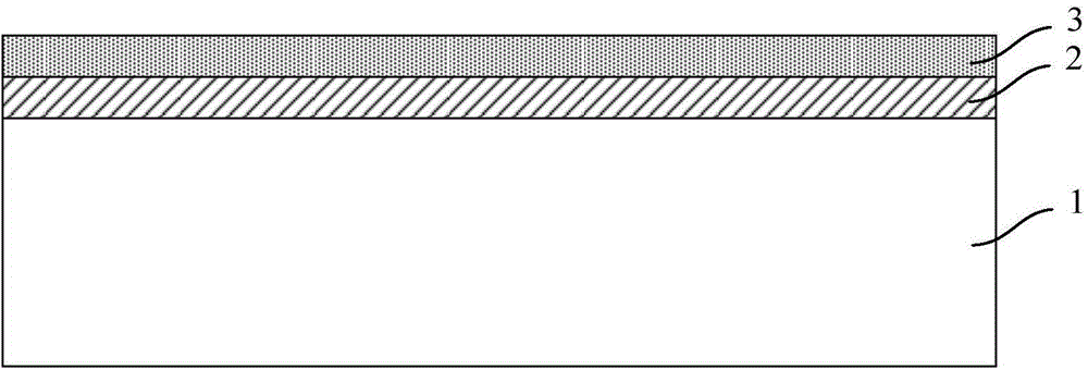
[0052] Step S1: providing an SOI substrate, the SOI substrate sequentially includes a silicon substrate, a buried oxide layer and a top layer of silicon from bottom to top;

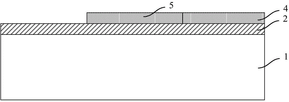
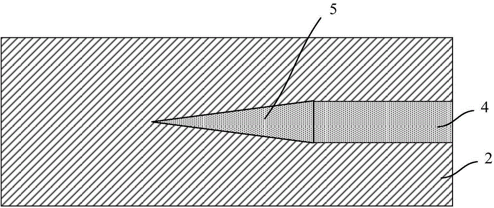
[0053] Step S2: Etching the top layer of silicon to form a silicon waveguide and a first tapered coupling structure connected to one end of the silicon waveguide; the longitudinal width of the first tapered coupling structure decreases linearly;

[0054] Step S3: forming a BCB cladding layer covering the silicon waveguide and the first tapered coupling structure on the surface of the buried oxide layer, and bonding a III-V family layer structure on the BCB cladding layer;

[0055] Step S4: Etching the III-V group layer structure to form a III-V group optical gain structure and a second tapered coupling structure connected to one end of the III-V group ...

Embodiment 2

[0072] The present invention also provides a coupler structure based on BCB bonding process, please refer to Figure 5 and Image 6 , which are respectively shown as a cross-sectional schematic diagram and a top view of the coupler structure based on the BCB bonding process of the present invention, the coupler structure includes:

[0073] A silicon substrate 1 and a buried oxide layer 2 formed on the silicon substrate 1;

[0074] The silicon waveguide 4 formed on the buried oxide layer 2 and the first tapered coupling structure 5 connected to one end of the silicon waveguide 4; the longitudinal width of the first tapered coupling structure 5 decreases linearly;

[0075] a BCB cladding layer 6 formed on the surface of the buried oxide layer 2 and covering the silicon waveguide 4 and the first tapered coupling structure 5;

[0076] The III-V group optical gain structure 8 formed on the surface of the BCB cladding layer 6 and the second tapered coupling structure 9 connected t...


PUM


Abstract

The invention provides a coupler structure based on BCB bonding technology and a production method thereof. The coupler structure is characterized in that a silicon substrate and a buried oxide layer disposed on the silicon substrate are provided; a silicon waveguide is disposed on the buried oxide layer, and a first cone-shaped coupling structure is connected with one end of the silicon waveguide; a BCB cladding is disposed on the surface of the buried oxide layer, and is used to cover the silicon waveguide and the first cone-shaped coupling structure; an III-V group optical gain structure is disposed on the surface of the BCB cladding, and a second cone-shaped coupling structure is connected with one end of the III-V group optical gain structure; the first cone-shaped coupling structure and the second cone-shaped coupling structure are in a reverse arrangement, and the projected parts on the horizontal plane are superposed with each other. The mixed integration of the III-V group optical gain structure and the silicon waveguide can be realized, and the mode conversion zone can be formed by adopting the reserve arrangement of the first cone-shaped coupling structure and the second cone-shaped coupling structure, and therefore the length of the coupling structure can be greatly shortened, and the coupling efficiency is high; when the thickness of the BCB cladding is changed, the change amplitude is small, and the coupling efficiency is more stable.

Description

technical field [0001] The invention belongs to the field of integrated optoelectronics, and relates to a coupler structure based on a BCB bonding process and a manufacturing method thereof. Background technique [0002] Silicon-based optical interconnect technology aims to use CMOS technology to produce and develop silicon photonic devices, and integrate silicon-based photonic devices and circuits on the same silicon chip. It is an inevitable way to develop large-capacity, high-performance parallel processing computer systems and communication equipment. Combining microelectronics technology and photonics technology to develop photoelectric hybrid integrated circuits. Introducing integrated optical circuits inside integrated circuits and between chips can not only take advantage of the advantages of fast optical interconnection, no interference, high density, and low power consumption, but also make full use of mature microelectronics technology, high-density integration, h...

Claims


Application Information

Patent Timeline
IPC IPC(8): G02B6/136G02B6/42G02B6/122
Inventor 盛振甘甫烷武爱民仇超王智琪
Owner 南通新微研究院
Why Eureka
Try Eureka