Structure of High Electron Mobility Light Emitting Transistor

A technology with high electron mobility and light-emitting transistors, which is applied in the direction of electric solid-state devices, circuits, electrical components, etc., and can solve problems such as uncontrollable brightness of light sources

Active Publication Date: 2018-07-24
黄智方
View PDF4 Cites 0 Cited by
  • Summary
  • Abstract
  • Description
  • Claims
  • Application Information

AI Technical Summary

Problems solved by technology

[0003] The invention provides a structure of a high electron mobility light-emitting transistor, which solves the problem that the brightness of the light source in the LED area is uncontrollable in the prior art

Method used


Image

  • Structure of High Electron Mobility Light Emitting Transistor
  • Structure of High Electron Mobility Light Emitting Transistor
  • Structure of High Electron Mobility Light Emitting Transistor

Examples


Embodiment Construction

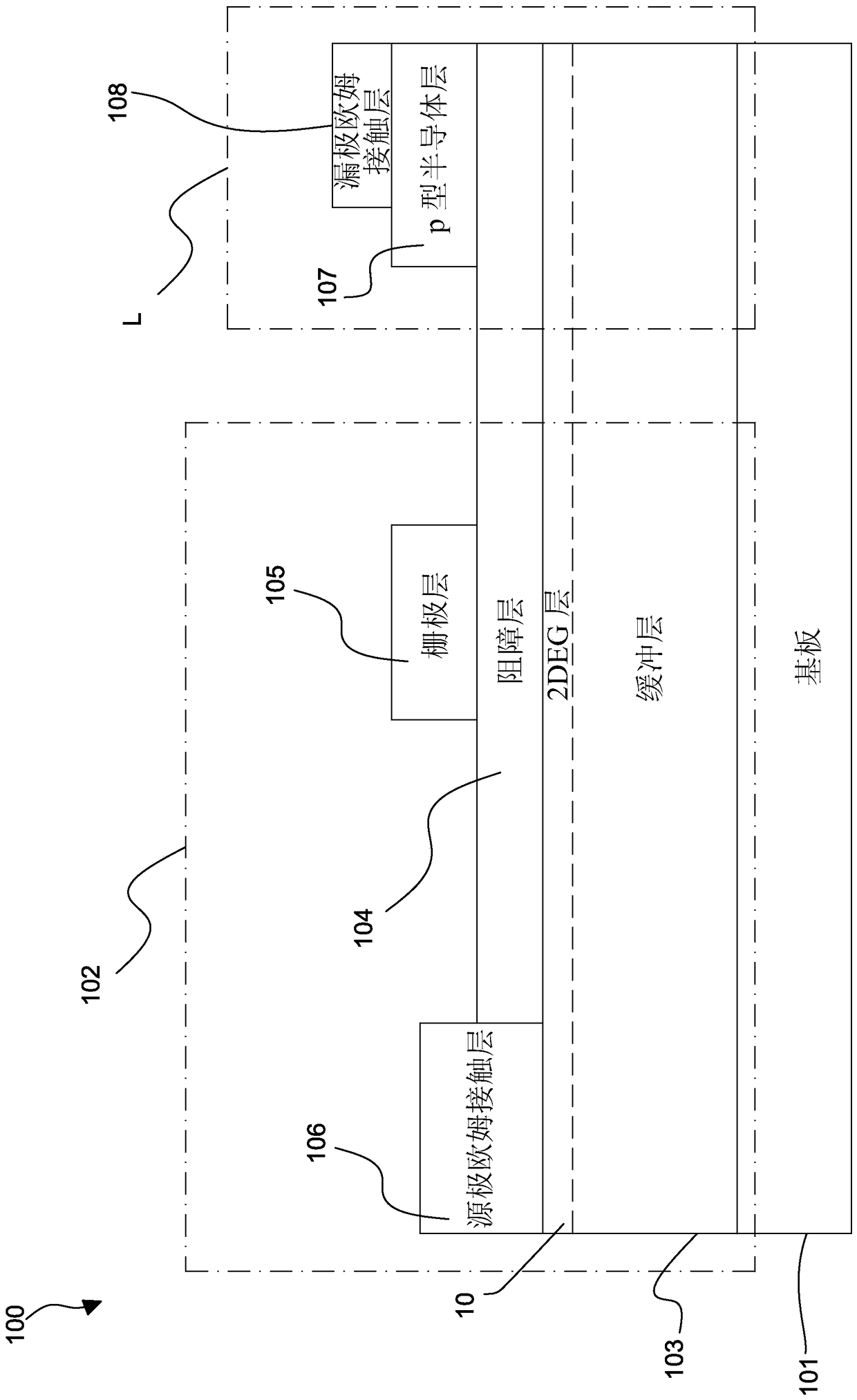
[0022] see figure 1 , figure 1 A schematic diagram showing an embodiment of the structure of the high electron mobility light-emitting transistor of the present invention. The structure 100 includes: a substrate 101 , a HEMT region 102 , and an LED region L.

[0023] The HEMT region 102 is disposed on the substrate 101 ; and the LED region L is also disposed on the substrate 101 . In this embodiment, the substrate 101 can be realized by a silicon (Si) substrate, or a gallium nitride substrate, or a sapphire substrate, or silicon carbide.

[0024] The structure 100 includes a buffer layer (Buffer) 103 and a barrier layer (Barrier) 104 . The buffer layer 103 is disposed on the substrate 101 ; and the barrier layer 104 is disposed on the buffer layer 103 , and the barrier layer 104 covers part of the buffer layer 103 .

[0025] In this embodiment, the HEMT region 102 includes: a gate (Gate) layer 105 and a source ohmic contact (Source ohmic contact) layer 106 . The gate la...


PUM


Abstract

The present invention provides a structure of a high electron mobility light-emitting transistor, which comprises: a substrate; a high mobility transistor (HEMT for short) region is arranged on the substrate; a gallium nitride light-emitting diode (GaN-LED, LED for short) region is arranged on On the substrate; wherein, both the HEMT region and the LED region have a two-dimensional electron gas layer, and the HEMT region is coupled to the LED region through the two-dimensional electron gas layer. The invention can generate light of different wavelengths, and can control the brightness of the light source in the LED area.

Description

technical field [0001] The present invention relates to a structure of a high electron mobility light-emitting transistor, especially a HEMT built-in LED structure. Background technique [0002] Aluminum Gallium Nitride / Gallium Nitride High Speed ​​Electron Mobility Transistor Field Effect Transistor (AlGaN / GaN HEMT) has extremely high advantages in high temperature, high frequency and high power applications; Because the direct bandgap of gallium nitride is 3.4eV, gallium nitride is also suitable for use in light-emitting devices. The wavelength range of light emitted by gallium nitride and its related ternary compounds It is very wide, ranging from green, blue to UV light, so light-emitting diodes of gallium nitride technology have been widely used. Contents of the invention [0003] The invention provides a structure of a high electron mobility light-emitting transistor, which solves the problem in the prior art that the brightness of the light source in the LED area c...

Claims


Application Information

Patent Timeline
Patent Type & Authority Patents(China)
IPC IPC(8): H01L27/15H01L29/778H01L33/06
Inventor 黄智方李奕辰张庭辅郑克勇王佑立吴浚宏杨伟臣邱绍谚
Owner 黄智方
Why Eureka
Try Eureka