
Semiconductor device and manufacturing method thereof, and electronic device

A manufacturing method, semiconductor technology, applied in semiconductor/solid-state device manufacturing, circuits, electrical components, etc., can solve problems such as burden, non-uniform critical dimensions, polysilicon is easy to be oxidized, etc., achieve good performance and yield, double pattern preparation method robust effect

Active Publication Date: 2016-08-03
SEMICON MFG INT (SHANGHAI) CORP
View PDF4 Cites 0 Cited by
  • Summary
  • Abstract
  • Description
  • Claims
  • Application Information

AI Technical Summary

Problems solved by technology

[0007] Among them, the spacer is widely used in self-aligned double patterning (Self-aligned double patterning, SADP), usually using lithography-etch-film deposition-etch-removal-nucleus-etch (Litho–Etch–filmdeposition-Etch–Strip -Etch.) method to prepare a semiconductor device, such as selecting amorphous carbon A-C and patterning it as the core (core) in the double pattern, then selecting a low-temperature deposition method to form a spacer layer on the A-C, and finally removing the A-C core, the method usually forms a cone-shaped core and also causes a burden when the dielectric anti-reflective coating (dielectric Anti-reflectivecoating, DRAC) is covered. In addition, there are odd-even (Even-odd) problems, such as odd-even critical dimensions Insufficient uniformity (Even-odd CDloading), in the prior art usually select polysilicon to replace described A-C to prepare polysilicon core, but polysilicon is easy to be oxidized in the preparation process, can cause odd-even number (Even-odd) problem likewise, make final The critical dimensions of the prepared fins are not uniform enough

Method used


Image

  • Semiconductor device and manufacturing method thereof, and electronic device
  • Semiconductor device and manufacturing method thereof, and electronic device
  • Semiconductor device and manufacturing method thereof, and electronic device

Examples


Embodiment 1

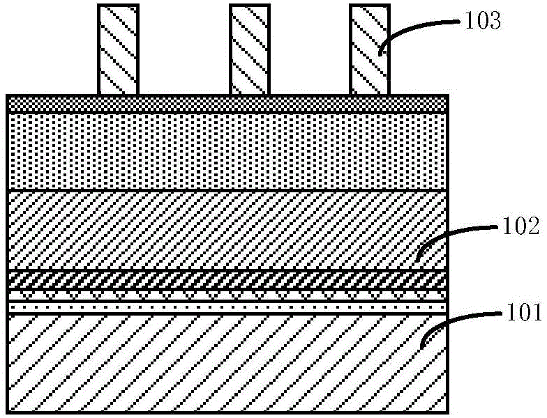
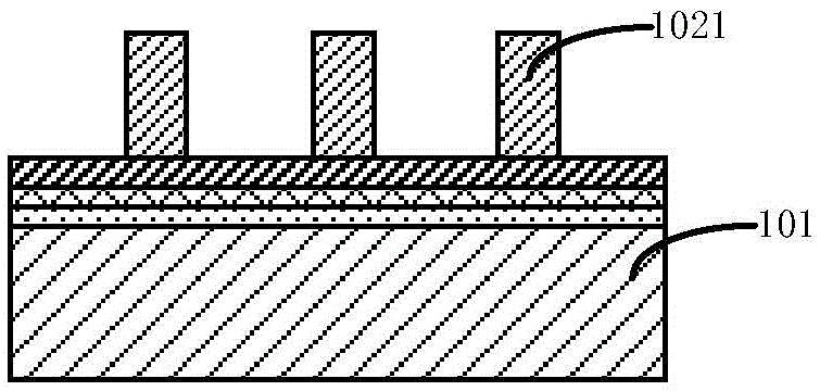
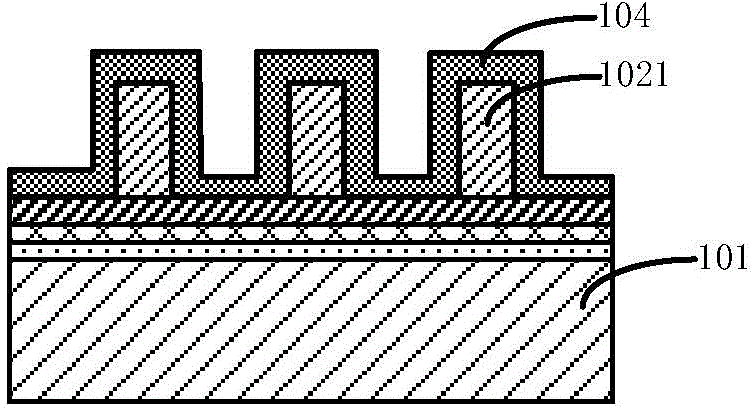
[0046] Attached below Figure 2a-2e The method of the present invention is further explained, wherein Figure 2a-2e It is a schematic diagram of a process of manufacturing a semiconductor device based on a dual pattern method in an embodiment of the present invention.

[0047] First, step 201 is performed to provide a semiconductor substrate 201, on which a doped oxide layer 206, amorphous silicon 202, and a patterned mask layer 203 are formed.

[0048] Specifically, such as Figure 2a As shown, the semiconductor substrate 201 may be at least one of the materials mentioned below: silicon, silicon-on-insulator (SOI), silicon-on-insulator (SSOI), silicon-germanium-on-insulator (S-SiGeOI) ), silicon germanium on insulator (SiGeOI) and germanium on insulator (GeOI), etc.

[0049] Optionally, an isolation structure may also be formed in the semiconductor substrate, and the isolation structure is a shallow trench isolation (STI) structure or a localized silicon oxide (LOCOS) isolation stru...

Embodiment 2

[0083] The present invention also provides a semiconductor device, which is prepared by using the method described in Embodiment 1. The pattern of the semiconductor device prepared by the method of the present invention has good uniformity and consistency, so as to further improve the performance and yield of the semiconductor device.

Embodiment 3

[0085] The present invention also provides an electronic device, including the semiconductor device described in Embodiment 2. Wherein, the semiconductor device is the semiconductor device described in Embodiment 2 or the semiconductor device obtained according to the manufacturing method described in Embodiment 1.

[0086] The electronic device of this embodiment may be any electronic product or equipment such as a mobile phone, a tablet computer, a notebook computer, a netbook, a game console, a TV, a VCD, a DVD, a navigator, a camera, a camcorder, a voice recorder, an MP3, an MP4, a PSP, etc. , Can also be any intermediate product including the semiconductor device. The electronic device of the embodiment of the present invention has better performance due to the use of the above-mentioned semiconductor device.


PUM


Abstract

The invention relates to a semiconductor device, a manufacturing method thereof, and an electronic device. The method includes step S1: providing a semiconductor substrate, on which a doped oxide layer is formed, and a number of dummy nuclei arranged at intervals are formed on the doped oxide layer; step S2: Depositing a layer of spacer material to cover the dummy core and the semiconductor substrate; step S3: choose CF 3 I and H 2 Etching the spacer material layer to form a spacer on the sidewall of the dummy core; step S4: removing the dummy core to obtain a fin pattern. The advantage of the present invention is that the preparation method of the double pattern is more robust, and the prepared FinFET has better performance and yield.

Description

Technical field [0001] The present invention relates to the field of semiconductor manufacturing. Specifically, the present invention relates to a semiconductor device, a manufacturing method thereof, and an electronic device. Background technique [0002] The improvement of integrated circuit performance is mainly achieved by continuously reducing the size of integrated circuit devices to increase its speed. At present, as the semiconductor industry pursuing high device density, high performance, and low cost has developed to smaller technology process nodes, challenges from manufacturing and design have promoted the development of three-dimensional designs such as FinFETs. [0003] Compared with the existing planar transistors, FinFET devices have more superior performance in channel control and reduction of shallow channel effects; among them, the planar gate structure is arranged above the channel, and the gate in FinFET Surrounding the fins can control static electricity from...

Claims


Application Information

Patent Timeline
Patent Type & Authority Applications(China)
IPC IPC(8): H01L21/336
Inventor 张海洋王冬江
Owner SEMICON MFG INT (SHANGHAI) CORP
Learn More