Formation method of CMOS (Complementary Metal Oxide Semiconductor) transistor

A technology of transistors and semiconductors, applied in semiconductor/solid-state device manufacturing, electrical components, circuits, etc., can solve the problems of low selectivity of PMOS work function layer, affecting the quality of other material layers, and low etching rate of PMOS work function layer, etc. Achieve the effect of high etching selectivity, avoiding damage, and high etching efficiency

Active Publication Date: 2016-08-03
SEMICON MFG INT (SHANGHAI) CORP
View PDF12 Cites 1 Cited by
  • Summary
  • Abstract
  • Description
  • Claims
  • Application Information

AI Technical Summary

Problems solved by technology

[0005] In the prior art, when removing the PMOS work function layer on the NMOS region, a wet etching process is generally used, which may encounter the problem that the etching rate of the PMOS work function layer is too low, or the selectivity of the PMOS work function layer is low. As a result, the PMOS work function layer on the NMOS transistor cannot be effectively removed or the quality of other material layers is affected, which affects the performance of the formed CMOS transistor

Method used


Image

  • Formation method of CMOS (Complementary Metal Oxide Semiconductor) transistor
  • Formation method of CMOS (Complementary Metal Oxide Semiconductor) transistor
  • Formation method of CMOS (Complementary Metal Oxide Semiconductor) transistor

Examples


Embodiment Construction

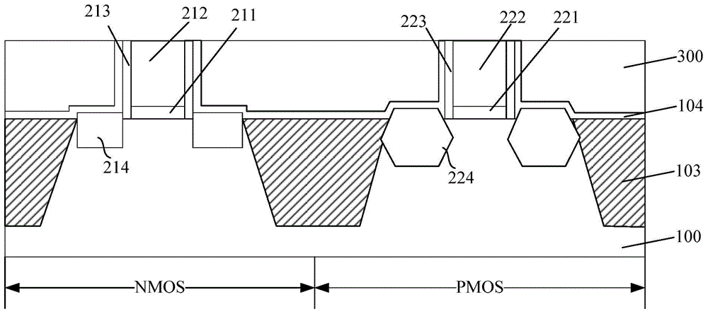
[0031] As mentioned in the background art, the performance of the CMOS transistors formed in the prior art needs to be further improved.

[0032] Currently, the material of the PMOS work function layer commonly used is TiN, and the material of the stop layer below the PMOS work function is generally TaN. The PMOS work function layer is usually removed by a wet etching process, and the etching solution used in the wet etching process is generally a mixed solution of ammonia and hydrogen peroxide (SC-1) or a mixed solution of hydrogen chloride and hydrogen peroxide ( SC-2), but the etching selectivity of the SC-1 solution for TiN is low, which is easy to cause over-etching, while the etching rate of the SC-2 solution for TiN is low, and when the thickness of the TiN layer is large, the etching less efficient.

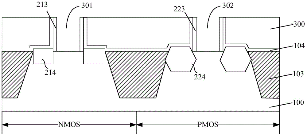
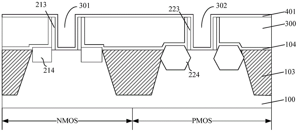
[0033] In the embodiment of the invention, an etching solution with higher etching efficiency and selectivity is used to etch the PMOS work function layer.

[0034] In ...


PUM

PropertyMeasurementUnit
quality scoreaaaaaaaaaa

Abstract

The invention relates to a formation method of CMOS (Complementary Metal Oxide Semiconductor) transistor, which comprises the steps of providing a semiconductor substrate, wherein the semiconductor substrate comprises an NMOS area and a PMOS area, the surface of the semiconductor substrate is provided with a dielectric layer, and the internal part of the dielectric layer is provided with a first groove and a second groove, forming a gate dielectric material layer, a stop layer and a PMOS work function layer at the wall surfaces of the first groove and the second groove and the surface of the dielectric layer, forming a mask layer which covers the PMOS area, removing the PMOS work function layer on the NMOS area, removing the mask layer, forming a metal layer which covers the NMOS area and the PMOS area and carrying out planarization processing. The step of removing the PMOS work function layer comprises the steps of firstly carrying out oxidation treatment on the PMOS work function layer on the NMOS area by adopting an ozone deionized aqueous solution, then carrying out etching treatment on the PMOS work function layer by adopting a hydrogen chloride deionized aqueous solution, repeating the above steps until the PMOS work function layer on the NMOS area is removed. The method provided by the invention can improve the performance of the CMOS transistor.

Description

technical field [0001] The invention relates to the technical field of semiconductors, in particular to a method for forming a CMOS transistor. Background technique [0002] With the continuous improvement of the integration level of semiconductor devices and the reduction of technology nodes, the traditional gate dielectric layer continues to become thinner, and the leakage of transistors increases accordingly, causing problems such as waste of power consumption of semiconductor devices. In order to solve the above problems, the prior art provides a solution of replacing the polysilicon gate with a metal gate. Among them, the "gate last" process is a main process for forming high-K metal gate transistors. [0003] The existing method for forming a high-K metal gate transistor using a gate-last process includes: providing a semiconductor substrate on which a dummy gate structure is formed and located on the semiconductor substrate and covering the dummy gate structure The ...

Claims


Application Information

Patent Timeline
Patent Type & Authority Applications(China)
IPC IPC(8): H01L21/8238
Inventor 刘佳磊
Owner SEMICON MFG INT (SHANGHAI) CORP
Why Eureka
Try Eureka