Method for detecting semiconductor polish wafer surface scratches

A detection method and semiconductor technology, applied in semiconductor/solid-state device testing/measurement, electrical components, circuits, etc., can solve problems such as corrosion, complex detection process, SiC wafer contamination, etc., and achieve low cost and small damage effects

Active Publication Date: 2016-08-17
INST OF PHYSICS - CHINESE ACAD OF SCI
View PDF6 Cites 6 Cited by
  • Summary
  • Abstract
  • Description
  • Claims
  • Application Information

AI Technical Summary

Problems solved by technology

Although this method can detect invisible scratches on the surface of SiC wafers, it has the following disadvantages: 1. The damage to SiC wafers is large, and the entire SiC wafer surface is corrode...

Method used


Image

  • Method for detecting semiconductor polish wafer surface scratches
  • Method for detecting semiconductor polish wafer surface scratches
  • Method for detecting semiconductor polish wafer surface scratches

Examples


Embodiment 1

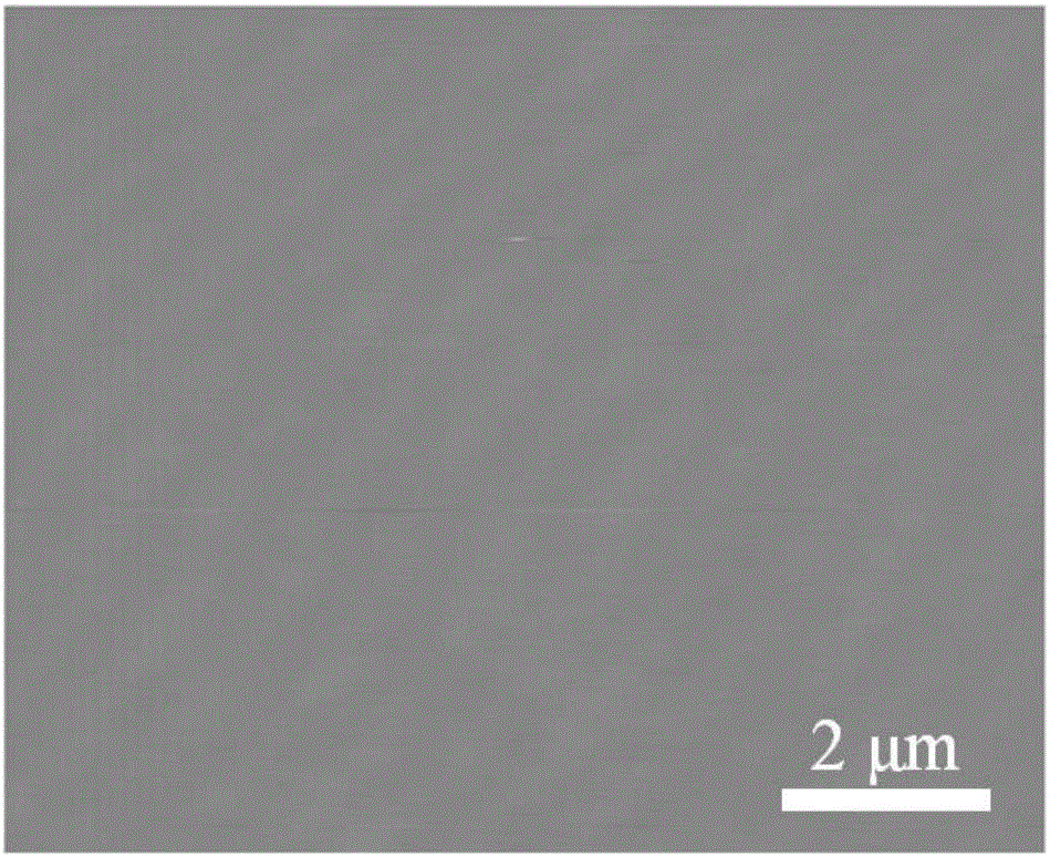
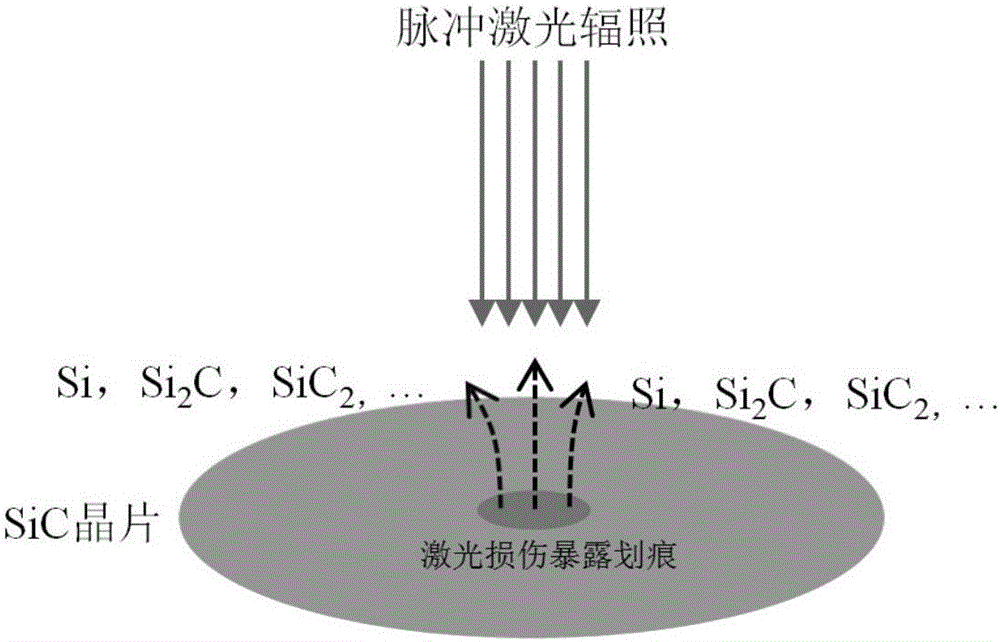
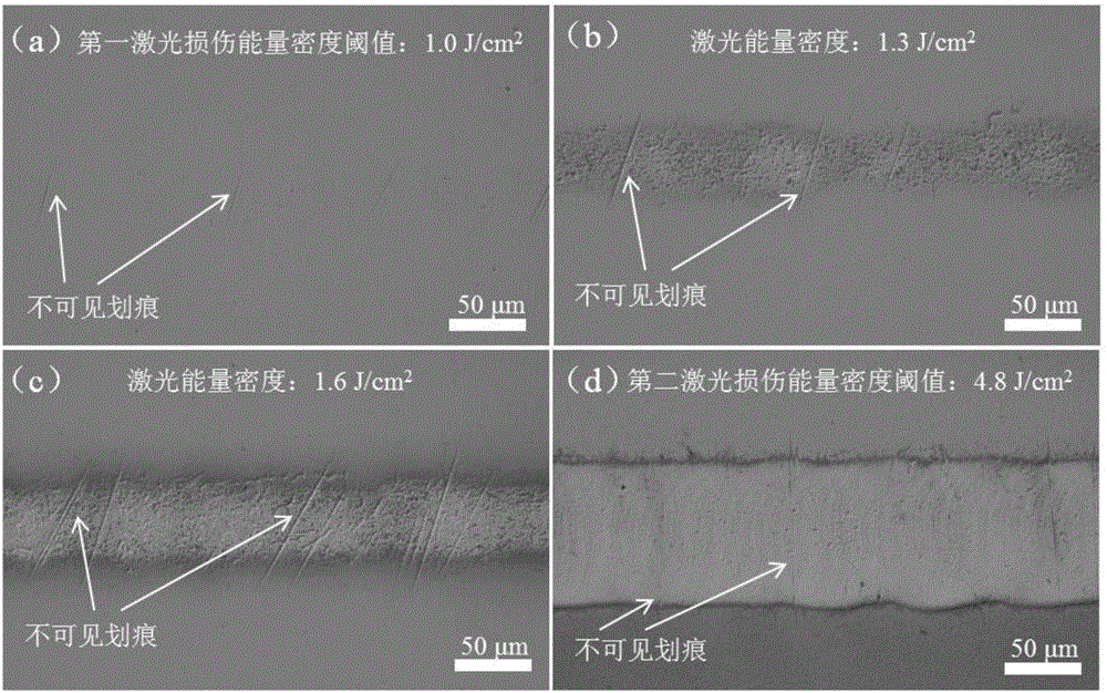
[0029] In this embodiment, a conductive 6H-SiC wafer doped with nitrogen (N) is taken as an example for illustration. figure 1 The atomic force microscope morphology of the nitrogen-doped 6H-SiC polished wafer surface after chemical mechanical polishing is shown. It can be seen that the scratches on the surface of the nitrogen-doped 6H-SiC polished wafer cannot be observed by the expensive atomic force microscope. The present embodiment provides a kind of detection method of the scratch on the conductive 6H-SiC polishing wafer surface of a kind of N doping, refer to below figure 2 and image 3 The method is described in detail. figure 2 A schematic diagram showing the detection method of SiC polished wafer surface scratches provided by the present invention, image 3 The optical microscope topography of the nitrogen-doped 6H-SiC polished wafer surface in the irradiated area is shown for different total laser irradiation energy densities. image 3 (a)-(d) corresponding to...

Embodiment 2

[0036] The present embodiment provides a kind of detection method of scratches on the surface of semi-insulating 4H-SiC wafer doped with vanadium (V), refer to below Figure 4 The method is described in detail. Figure 4 The optical microscope topography of vanadium-doped 4H-SiC polished wafer surface in the irradiated area is shown for different total laser irradiation energy densities. Figure 4 (a)-(d) corresponding to the total laser irradiation energy density is 1.6J / cm 2 、2.1J / cm 2 , 2.5J / cm 2 and 5.3J / cm 2 . The detection method of the vanadium-doped 4H-SiC polished wafer surface scratch of the present embodiment comprises the following steps:

[0037] 1) The size to be detected is 1×1cm 2 The vanadium-doped semi-insulating 4H-SiC wafer was ultrasonically cleaned with acetone, absolute ethanol and deionized water in sequence, and finally the cleaned silicon carbide wafer was blown dry with nitrogen.

[0038] 2) Irradiating the cleaned vanadium-doped 4H-SiC wafer ...


PUM

PropertyMeasurementUnit
Wavelengthaaaaaaaaaa
Diameteraaaaaaaaaa

Abstract

The invention provides a method for detecting semiconductor polish wafer surface scratches. The detection method comprises the following steps that 1, a semiconductor polish wafer is irradiated by means of a pulse laser; 2, the semiconductor polish wafer surface subjected to pulse laser irradiation is observed with a microscope, wherein the total irradiation energy density of the pulse laser is between a first damage energy density threshold value and a second damage energy density threshold value. The detection method is high in speed, low in cost, small in damage to the wafer, free of pollution and capable of being widely applied to rapid detection on the surface scratches of semiconductor polish wafer products.

Description

technical field [0001] The invention relates to a method for detecting scratches on the surface of a wafer, in particular to a method for detecting scratches on the surface of a semiconductor polished wafer. Background technique [0002] During the preparation of semiconductor wafers, the semiconductor is usually cut mechanically, and then the surface of the cut wafer is roughly ground, finely ground, and chemically and mechanically polished to meet the requirements of epitaxy. However, there is often a damaged layer on the surface of a chemically mechanically polished semiconductor wafer, and scratches in the damaged layer will have negative effects on the quality of subsequent homogeneous or heteroepitaxially grown materials and device performance. [0003] Currently, defects larger than a few microns in size on the surface of semiconductor wafers can be easily identified with the aid of an optical microscope. However, scratches with a width smaller than micron scale (we ...

Claims


Application Information

Patent Timeline
IPC IPC(8): H01L21/66
CPCH01L22/12H01L22/24
Inventor 郭丽伟甘弟陈小龙
Owner INST OF PHYSICS - CHINESE ACAD OF SCI
Why Eureka
Try Eureka