GaN-based white-light LED and preparation method

A white light and blue light technology, applied in electrical components, circuits, semiconductor devices, etc., can solve the problems of high cost and complex methods of generating white light, and achieve the effects of high conversion efficiency, low cost and simple preparation process

Active Publication Date: 2016-08-17
INST OF SEMICONDUCTORS - CHINESE ACAD OF SCI
View PDF2 Cites 19 Cited by
  • Summary
  • Abstract
  • Description
  • Claims
  • Application Information

AI Technical Summary

Problems solved by technology

Using a variety of monochromatic light mixing methods, because the driving voltage, light output, temperature characteristics and lifespan of LED light-emitting diodes of different colors are different, so the meth

Method used


Image

  • GaN-based white-light LED and preparation method
  • GaN-based white-light LED and preparation method

Examples


preparation example Construction

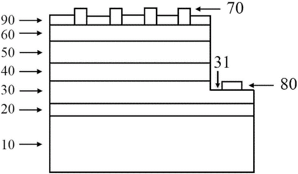
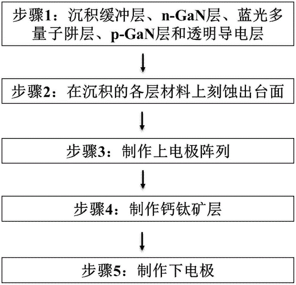
[0042] see figure 2 and refer to figure 1 As shown, the present invention also provides a method for preparing a GaN-based white light LED, comprising the following steps:

[0043]Step 1: sequentially fabricate a buffer layer 20, an n-GaN layer 30, a blue light multi-quantum well layer 40, a p-GaN layer 50 and a transparent conductive layer 60 on a substrate 10 by means of MOCVD, the substrate 10 The material is sapphire, SiC or Si, the material of the blue multi-quantum well layer 40 is at least two of InGaN, InAlN, AlGaN, AlInGaN or InGaAlP, and the material of the transparent conductive layer 60 is ITO, FTO or silver nanowire ;

[0044] Step 2: Etching downward from the side above the transparent conductive layer 60, the etching depth reaches into the n-GaN layer 30, and forming a mesa 31 on one side of the n-GaN layer 30;

[0045] Step 3: making an upper electrode array 70 on the transparent conductive layer 60;

[0046] Step 4: Make a perovskite layer 90 on the top o...

Embodiment 1

[0049] A low-temperature GaN buffer layer was deposited on the sapphire substrate by metal-organic chemical vapor deposition (MOCVD). An approximately 2 μm thick n-GaN layer is deposited on the GaN buffer layer. A blue light multiple quantum well layer is deposited on the n-GaN layer. A layer of about 2 μm-GaN is deposited on the blue MQW layer. Perform photolithography and etching to etch part of the area down to the n-GaN layer. A transparent conductive layer is deposited on the unetched p-GaN layer with a thickness of 200-500 nm by electron beam evaporation. A Ti / Au metal electrode array was deposited on the transparent conductive layer with EB. Ti / Au metal electrodes are deposited on the n-GaN layer exposed after etching. 0.9 mol of PbBr2, 0.1 mol of PbI2 and 1 mol of CH 3 NH 3 Br mixed, dissolved in 2ml DMF, fully dissolved and filtered. The perovskite layer is deposited on the transparent conductive layer by gas-assisted spin coating, the speed of the homogenizer ...


PUM

PropertyMeasurementUnit
Thicknessaaaaaaaaaa
Thicknessaaaaaaaaaa

Abstract

A GaN-based white-light LED comprises a substrate, a buffer layer, an n-GaN layer, a blue-light multiple quantum well layer, a p-GaN layer, a transparent conducting layer, an upper electrode array, a lower electrode and a perovskite layer. The buffer layer is made on the substrate, the n-GaN layer is made on the buffer layer, and a table top is formed on one side on the n-GaN layer; the blue-light multiple quantum well layer is made on the other side of the table top of the n-GaN layer, the p-GaN layer is made on the blue-light multiple quantum well layer, the transparent conducting layer is made on the p-GaN layer, the upper electrode array is made on the transparent conducting layer, and the lower electrode is made on the table top of the n-GaN layer; the perovskite layer is made on the transparent conducting layer and located in gaps of the electrode array. According to the GaN-based white-light LED, a mature GaN-based LED technology is combined with a novel perovskite materials, and the white-light LED which is low in cost and efficient is made out.

Description

technical field [0001] The invention belongs to the field of semiconductor devices, and relates to a high-efficiency GaN-based white light LED and a preparation method. Background technique [0002] LED light source has the advantages of using low-voltage power supply, less energy consumption, strong applicability, high stability, short response time, no pollution to the environment, and multi-color light emission. It is foreseeable that in the near future, white LEDs will enter the family to replace the existing lighting. [0003] There are usually two methods for white LEDs. The first is to use blue LEDs and yellow phosphors to form white light; the second is to mix multiple monochromatic lights. Both approaches have successfully produced white light devices. The most common and mature one is to apply a layer of yellow phosphor on the blue chip to make the blue light and yellow light mix into white light, so the material of the phosphor has a great influence on the atten...

Claims


Application Information

Patent Timeline
IPC IPC(8): H01L33/32H01L33/06H01L33/50H01L33/00
CPCH01L33/0075H01L33/06H01L33/32H01L33/502
Inventor 袁国栋王乐段瑞飞李晋闽王军喜黄芳吴瑞伟王克超
Owner INST OF SEMICONDUCTORS - CHINESE ACAD OF SCI
Why Eureka
Try Eureka