Perovskite photoelectric device and preparation method thereof and perovskite material

A technology of perovskite materials and optoelectronic devices, which is applied in the fields of electric solid state devices, semiconductor/solid state device manufacturing, photovoltaic power generation, etc. Improve efficiency and life, solve film discontinuity, and achieve the effect of energy transfer

Active Publication Date: 2016-08-24
NANJING UNIV OF TECH
View PDF5 Cites 24 Cited by
  • Summary
  • Abstract
  • Description
  • Claims
  • Application Information

AI Technical Summary

Problems solved by technology

However, the problem of poor film-forming quality and stability of three-dimensional perovskite materials has become an important factor limiting the performance of light-emitting devices and photovoltaic devices. Although two-dimensional layered perovskite films have good film-forming properties and stability, However, the photoluminescence quantum efficiency of the thin film is low, and the device needs to be luminescent at low temperature.

Method used


Image

  • Perovskite photoelectric device and preparation method thereof and perovskite material
  • Perovskite photoelectric device and preparation method thereof and perovskite material
  • Perovskite photoelectric device and preparation method thereof and perovskite material

Examples


preparation example Construction

[0105] Example 1AX 1 preparation.

[0106] AX 1 The preparation method is as follows: dissolve A in tetrahydrofuran, then add hydriodic acid to react for 60 minutes, make the pH value of the reaction solution 4, remove the solvent by rotary evaporation to obtain a solid powder, wash the obtained powder with ether and filter three times to obtain it, as follows with C 10 h 7 CH 2 NH 3 The synthetic method of I is example, at first arylamine C 10 h 7 CH 2 NH 2 Dissolve in tetrahydrofuran, then add hydriodic acid to react for 60 minutes, make the pH of the reaction solution 4, remove the solvent by rotary evaporation to obtain a solid powder, wash and filter the obtained powder with ether three times to obtain a white C 10 h 7 CH 2 NH 3 I powder. According to this method, the synthesis of C 10 h 7 CH 2 NH 3 Br, C 10 h 7 CH 2 NH 3 Cl, C 6 h 5 CH 2 NH 3 I.C 6 h 5 (CH 2 ) 2 NH 3 I.C 6 h 5 (CH 2 ) 4 NH 3 I.

Embodiment 2

[0107] Example 2 Preparation of layered perovskite material.

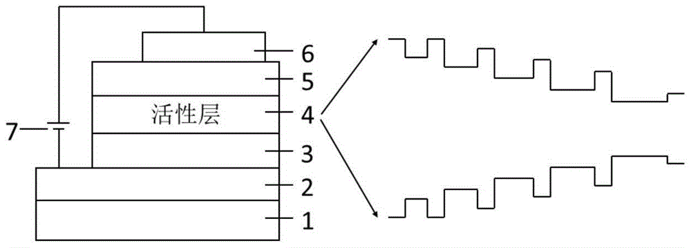
[0108] Will C 10 h 7 CH 2 NH 3 I, NH 2 CH=NH 2 I and PbI 2 Prepare the precursor solution at a molar ratio of 2:1:2, spin-coat the above precursor solution on the substrate, and obtain a layered perovskite film with a multi-quantum well structure (referred to as NFPI for short) after annealing. 7 ).

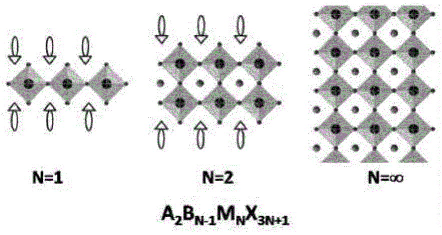
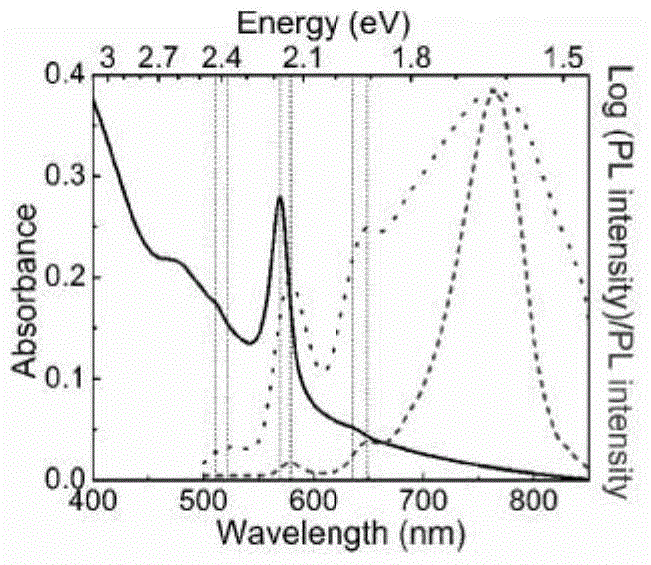
[0109] Such as image 3 Shown, NFPI 7 The film has an obvious exciton absorption peak at 569nm, indicating that the main existence of this perovskite material is the material of N=2 ((C 10 h 7 CH 2 NH 3 ) 2 (NH 2 CH=NH 2 )[Pb 2 I 7 ]), and it can be seen that NFPI 7 The film contains N=1((C 10 h 7 CH 2 NH 3 ) 2 PB 4 ) and N=4((C 10 h 7 CH 2 NH 3 ) 2 (NH 2 CH=NH 2 ) 3 [Pb 4 I 13 ]) (X.Hong et al., Dielectric Confinement Effect on Excitons in PbI 4 -Based Layered Semiconductors.Phys.Rev.B.45,6961–6964(1992);K.Tanaka et al.,Bandgap and exciton binding energies inlead-iodide-based natura...

Embodiment 3

[0110] Example 3 Preparation of layered perovskite material.

[0111] Will C10 h 7 CH 2 NH 3 I, NH 2 CH=NH 2 Br and PbI 2 Prepare the precursor solution at a molar ratio of 2:1:2, spin-coat the above precursor solution on the substrate, and obtain a layered perovskite film with a self-assembled multiple quantum well structure (referred to as NFPI for short) after annealing. 6 B).

[0112] Such as Figure 8 Shown, NFPI 6 B thin film has obvious exciton absorption peak at 557nm, and photoluminescence peak is mainly located at 750nm, with the NFPI of embodiment 2 7 Films are similar. Figure 9 for NFPI 6 The surface morphology of the B film, indicating that NFPI 6 B thin film has good film-forming properties, and the root mean square roughness of the surface is only 2.6nm. Figure 10 for NFPI 6 From the TCSPC test results of the B film, it can be seen that the PL lifetime of the film is longer at 750nm, reaching 30ns.


PUM

PropertyMeasurementUnit
emission peakaaaaaaaaaa
external quantum efficiencyaaaaaaaaaa
internal quantum efficiencyaaaaaaaaaa

Abstract

The invention discloses a perovskite photoelectric device, which comprises a substrate, electrode layers and a function layer. One electrode layer is arranged on the surface of the substrate; the function layer is arranged between the electrode layers; and the function layer at least comprises a perovskite layer, wherein the perovskite layer is a perovskite material having a self-assembled multiple-quantum-well structure. By adjusting material components, controllable adjustment of width of multiple quantum wells and effective energy transfer between the multiple quantum wells can be realized; emitting color can be near ultraviolet, visible light and near infrared light; and the problems of discontinuity and poor stability of an existing perovskite material thin film can be solved effectively. The perovskite photoelectric device is simple in process and low in cost, and is suitable for being widely applied to industrial production of large-area, low-cost, flexible substrate and high-performance devices. The invention also discloses the perovskite material, which can be used for photoluminescence, electroluminescence, photovoltaic and thin film transistor devices.

Description

technical field [0001] The invention relates to a device based on a perovskite material with a self-assembled multiple quantum well structure, a preparation method, and a perovskite material with a self-assembled multiple quantum well structure. Background technique [0002] Since the beginning of the 21st century, with the development of human society and the improvement of living standards, energy and the environment are facing severe challenges. The development of new equipment with low power consumption and green environmental protection has become an urgent need for people. In recent years, an organic-inorganic hybrid perovskite material, which has abundant and cheap raw materials and can be used for low-cost and large-area optoelectronic devices by low-temperature solution process, has aroused the interest of researchers in related fields all over the world. Perovskite thin film is one of the few crystalline thin films with excellent charge transport performance. At th...

Claims


Application Information

Patent Timeline
Patent Type & Authority Applications(China)
IPC IPC(8): H01L51/42H01L51/46H01L51/48H01L51/00H01L51/50H01L51/54H01L51/56B82Y30/00B82Y40/00
CPCB82Y30/00B82Y40/00H10K71/164H10K85/30H10K30/30H10K50/14H10K50/11H10K71/00Y02E10/549Y02P70/50H10K85/1135H10K85/60H10K30/151H10K30/20H10K2102/103H10K85/50H10K30/00H10K85/611H10K30/10H10K30/81H10K50/805H10K85/623H10K85/652H10K85/654H01S5/36
Inventor 王建浦王娜娜葛睿黄维
Owner NANJING UNIV OF TECH
Why Eureka
Try Eureka