Red and yellow light emitting diode epitaxial wafer and preparation method thereof

A technology of light-emitting diodes and epitaxial wafers, which is applied in the direction of electrical components, circuits, semiconductor devices, etc., can solve the problems of low luminous efficiency, achieve the effect of improving luminous efficiency and increasing the recombination probability

Active Publication Date: 2016-08-31
HC SEMITEK SUZHOU
View PDF6 Cites 13 Cited by
  • Summary
  • Abstract
  • Description
  • Claims
  • Application Information

AI Technical Summary

Problems solved by technology

[0006] In order to solve the problem of low luminous efficiency in the prior art, an embodiment of the pre

Method used


Image

  • Red and yellow light emitting diode epitaxial wafer and preparation method thereof
  • Red and yellow light emitting diode epitaxial wafer and preparation method thereof
  • Red and yellow light emitting diode epitaxial wafer and preparation method thereof

Examples


Embodiment 1

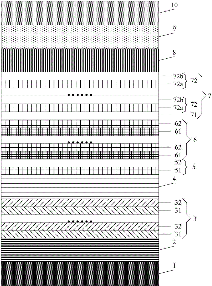
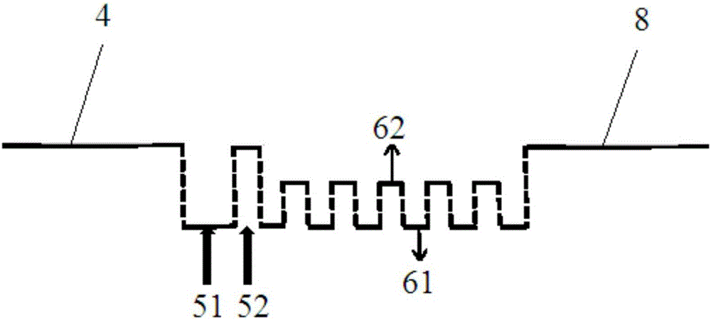
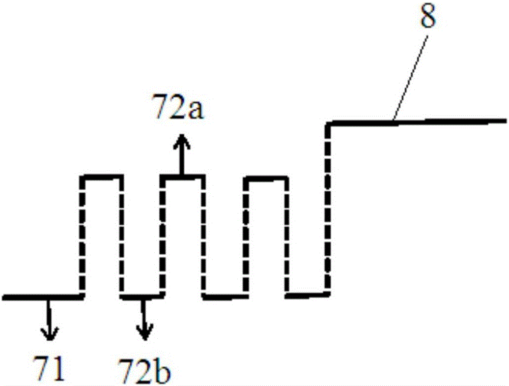
[0035] An embodiment of the present invention provides a red and yellow light emitting diode epitaxial wafer, see figure 1 The red and yellow light emitting diode epitaxial wafer includes an N-type substrate 1, and an N-type buffer layer 2, an N-type reflective layer 3, an N-type confinement layer 4, an electron blocking layer 5, Multi-quantum well layer 6 , hole adjustment layer 7 , P-type confinement layer 8 , P-type current spreading layer 9 , and P-type ohmic contact layer 10 .

[0036] In this embodiment, the N-type substrate 1 is a GaAs substrate; the N-type buffer layer 2 is a GaAs layer; the N-type reflective layer 3 includes alternately stacked AlAs layers 31 and AlGaAs layers 32; the N-type confinement layer 4 is an AlInP layer The electron blocking layer 5 includes AlGaInP layers 51 and AlInP layers 52; the multi-quantum well layer 6 includes alternately stacked quantum well layers 61 and quantum barrier layers 62 (the quantum well layers and the quantum barrier lay...

Embodiment 2

[0080] The embodiment of the present invention provides a method for preparing a red-yellow light-emitting diode epitaxial wafer, which is suitable for preparing the red-yellow light-emitting diode epitaxial wafer provided in Example 1, see image 3 , the preparation method comprises:

[0081] Step 201: forming an N-type buffer layer on an N-type substrate.

[0082] In this embodiment, the N-type substrate is a GaAs substrate; the N-type buffer layer is a GaAs layer.

[0083] Specifically, the N-type substrate can be a 2 or 4-inch 100-plane-offset A+5° GaAs substrate.

[0084] Optionally, the thickness of the N-type substrate may be 340-360 μm.

[0085] Optionally, the doping impurity of the N-type substrate can be silicon element, and the doping concentration of the N-type substrate 1 can be 10 -18 ~2*10 -18 cm -3 .

[0086] Specifically, the growth conditions of the N-type buffer layer may be as follows: the growth temperature is 640-660° C., the flow rate of TMGa (tri...


PUM

PropertyMeasurementUnit
Thicknessaaaaaaaaaa
Thicknessaaaaaaaaaa
Thicknessaaaaaaaaaa

Abstract

The present invention discloses a red and yellow light emitting diode epitaxial wafer and a preparation method thereof, belonging to the field of the semiconductor technology. The epitaxial wafer comprises a N-type substrate, a N-type buffer layer, a N-type reflection layer, a N-type restriction layer, an electronic blocking layer, a multiple quantum well layer, a cavity regulation layer, a P-type restriction layer, a P-type current extension layer and a P-type ohmic contact layer. The electronic blocking layer includes an AlGaInP layer and an AlInP layer; the cavity regulation layer includes a first sublayer and at least two second sublayers; the first sublayer is a non-doped AlInP layer, and a second sublayer includes a P-type doped AlInP layer and a non-doped AlInP layer; and the dosage concentration of the P-type doped AlInP layer is smaller than the P-type doped AlInP layer of the P-type restriction layer. The electronic blocking layer is used for delaying electrons to reach the multiple quantum well layer, and the cavity regulation layer is configured to allow the cavities to be uniformly distributed in the regions closed to the multiple quantum well layer so as to increase the recombination rate of the electrons and the cavities and improve the luminous efficiency of the light emitting diode.

Description

technical field [0001] The invention relates to the technical field of semiconductors, in particular to a red-yellow light-emitting diode epitaxial wafer and a preparation method thereof. Background technique [0002] Red and yellow high-brightness AlGaInP-based light-emitting diodes (Light Emitting Diode, referred to as LEDs) have the advantages of small size, long life, and low power consumption. Broad application prospects. [0003] AlGaInP LED epitaxial wafer includes N-type substrate, N-type buffer layer, N-type reflective layer, N-type confinement layer, multiple quantum well layer, P-type confinement layer, P-type current spreading layer, P-type ohmic contact layer from bottom to top . [0004] In the process of realizing the present invention, the inventor finds that there are at least the following problems in the prior art: [0005] The volume and mass of electrons are smaller than holes, so the mobility and mobility of electrons are better than holes. Most of t...

Claims


Application Information

Patent Timeline
IPC IPC(8): H01L33/14H01L33/30H01L33/00
CPCH01L33/0062H01L33/14H01L33/145H01L33/30
Inventor 王世俊邢振远李彤董耀尽
Owner HC SEMITEK SUZHOU
Why Eureka
Try Eureka