
Preparation method for CdS or CdSe single-crystal nanowire array

A single crystal nanowire array technology, applied in the field of preparation of CdS or CdSe single crystal nanowire arrays, can solve the problems of low crystallinity, complex steps, low yield, etc., and achieve high crystallinity, simple steps, and low defects. Effect

Active Publication Date: 2016-09-07
TECHNICAL INST OF PHYSICS & CHEMISTRY - CHINESE ACAD OF SCI
View PDF3 Cites 2 Cited by
  • Summary
  • Abstract
  • Description
  • Claims
  • Application Information

AI Technical Summary

Problems solved by technology

However, in addition to their respective advantages, the above methods often have different degrees of limitations and deficiencies.
For example, although the gas-liquid-solid (VLS) method is simple, it requires the assistance of additional metal catalysts, and the surface and structure of the prepared nanomaterials will be doped with auxiliary metal components.
Although the structure and composition of the material can be precisely controlled by the MBE method, the method has high cost, low output and complicated steps.
For the solution method, the prepared materials often have the disadvantage of low crystallinity

Method used


Image

  • Preparation method for CdS or CdSe single-crystal nanowire array
  • Preparation method for CdS or CdSe single-crystal nanowire array
  • Preparation method for CdS or CdSe single-crystal nanowire array

Examples


Embodiment 1

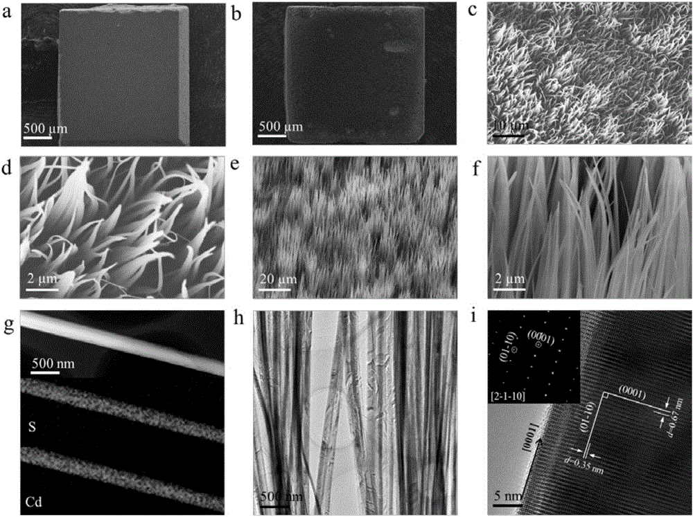
[0035] 1) Put the CdS single wafer into the ceramic sheet, and then place the ceramic sheet in the high-temperature heating zone of the tube furnace; the purity of the hexagonal CdS single wafer is 99.9%;

[0036] 2) Turn on the mechanical pump, vacuumize the tube furnace that puts the ceramic sheet, and reduce the pressure in the tube furnace to 0.1Pa, then feed argon and hydrogen into the tube furnace at a rate of 40mL / min. Mixed gas (the volume ratio of argon and hydrogen is 95:5), so that the pressure in the tube furnace is maintained at 200Pa; then the tube furnace is heated to 750 °C at a rate of 25 °C / min, and the pressure is 200 Pa. The reaction was carried out for 30 minutes; after the reaction, the tube furnace was naturally cooled to room temperature, and the samples were taken out. The sample is a CdS single crystal nanowire array.

[0037] Depend on figure 1 Figure i in the figure shows that the HRTEM image and SAED image of the CdS single crystal nanowire array...

Embodiment 2

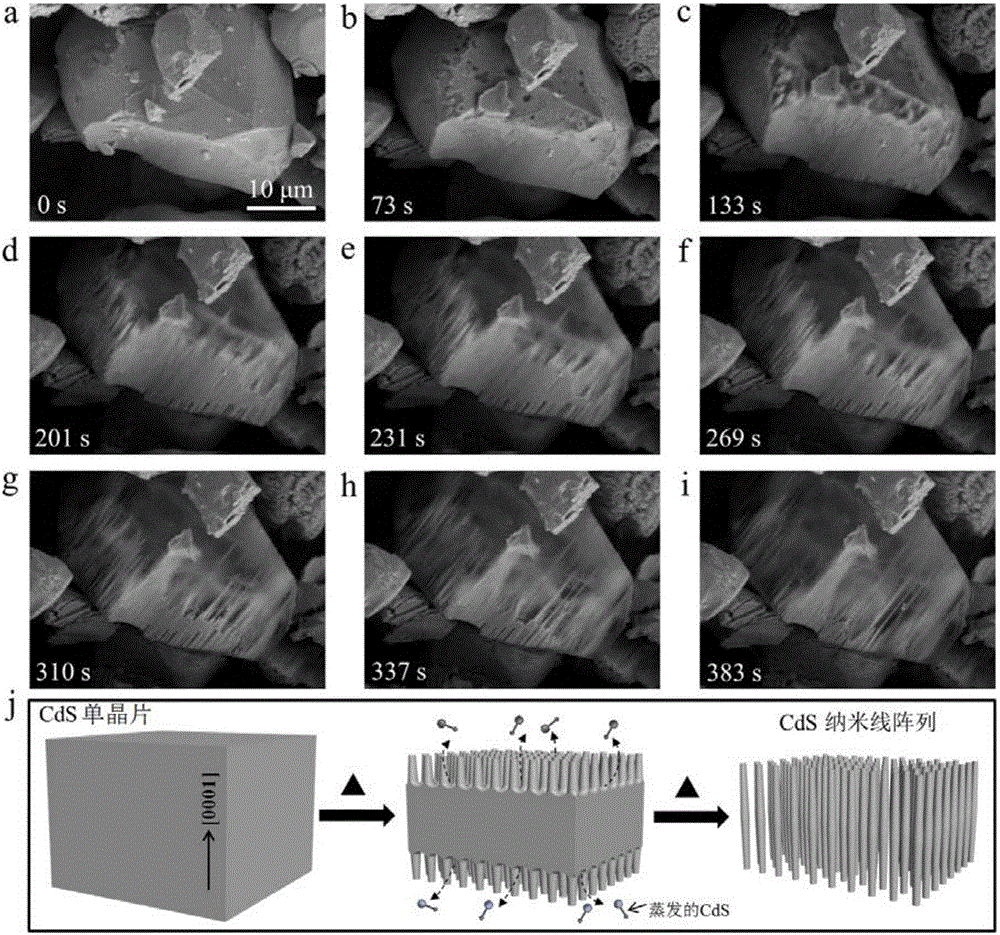
[0039] 1) putting CdS powder particles with a particle size greater than 5 μm into a ceramic sheet, and then placing the ceramic boat in a high-temperature heating zone of a tube furnace; the purity of the CdS powder particles is 99.9%;

[0040]2) Turn on the mechanical pump, vacuumize the tube furnace that puts the ceramic sheet, and reduce the pressure in the tube furnace to 0.1pa, then feed argon and hydrogen into the tube furnace at a rate of 40mL / min. Mixed gas (the volume ratio of argon and hydrogen is 95:5), so that the pressure in the tube furnace is maintained at 200Pa; then the tube furnace is heated to 750 °C at a rate of 25 °C / min, and the pressure is 200 Pa. The reaction was carried out for 30 minutes; after the reaction, the tube furnace was naturally cooled to room temperature, and the samples were taken out. The sample is a CdS single crystal nanowire array.

[0041] combine figure 2 Figures a to i in the figure show that the time-resolved ESEM images during...

Embodiment 3

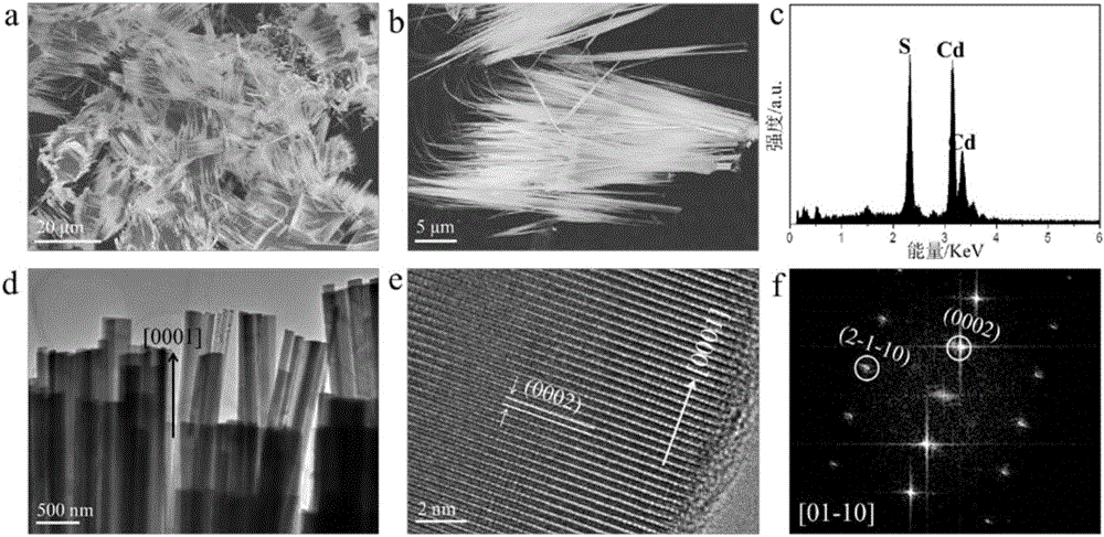
[0043] 1) putting CdSe powder particles with a particle size greater than 5 μm into a ceramic sheet, and then placing the ceramic boat in a high-temperature heating zone of a tube furnace; the purity of the CdSe powder particles is 99.9%;

[0044] 2) Turn on the mechanical pump, vacuumize the tube furnace that puts the ceramic sheet, and reduce the pressure in the tube furnace to 0.1Pa, then feed argon and hydrogen into the tube furnace at a rate of 40mL / min. Mixed gas (the volume ratio of argon and hydrogen is 95:5), so that the pressure in the tube furnace is maintained at 200Pa; then the tube furnace is heated to 650 °C at a rate of 20 °C / min, and the pressure is 200 Pa. The reaction was carried out for 30 minutes; after the reaction, the tube furnace was naturally cooled to room temperature, and the samples were taken out. The sample is a CdSe single crystal nanowire array.

[0045] combined by Figure 4 Figure i shows that the HRTEM image and SAED image of the CdSe sing...


PUM

PropertyMeasurementUnit
particle diameteraaaaaaaaaa
lattice spacingaaaaaaaaaa

Abstract

The invention discloses a preparation method for a CdS or CdSe single-crystal nanowire array. The preparation method comprises the following steps: placing CdS or CdSe solid body on a substrate; then, placing the substrate in a high-temperature heating area of a tube furnace; vacuumizing the tube furnace into which the substrate is placed and introducing a protective gas; raising the temperature of the tube furnace, maintaining the pressure intensity in the tube furnace at 10 to 2,000 Pa, reacting for 0.1 to 2 hours, and naturally decreasing the temperature of the tube furnace to room temperature after the reaction is ended. The preparation method is low in cost, high in controllability and simple in steps; the CdS single-crystal nanowire array or the CdSe single-crystal nanowire array prepared by the preparation method are arranged tidily and are consistent in crystal orientation, high in crystallinity degree and low in defect rate, show excellent photoelectric properties, and have a very important research value and a very important application prospect in the aspects of nano-scale optoelectronic devices, solar cells, photocatalysis, bio-sensing and the like.

Description

technical field [0001] The invention relates to the technical field of semiconductor nanometer materials. More specifically, it relates to a method for preparing a CdS or CdSe single crystal nanowire array. Background technique [0002] Semiconductor nanomaterials have attracted extensive research interest due to their low-dimensional structures and unique physical and chemical properties. Taking CdS as an example, many experiments and theoretical studies have shown that CdS semiconductor nanomaterials have great application prospects in piezoelectric electronics, optoelectronics, mechanics, and energy storage. Since the performance of nanodevices largely depends on the diameter, length, crystallinity, structure, and chemical composition of nanomaterials, how to achieve strict control of these parameters has become a major research topic in the application of nanomaterials. [0003] In the past few decades, the preparation technology of nanomaterials has made great progres...

Claims


Application Information

Patent Timeline
Patent Type & Authority Applications(China)
IPC IPC(8): C30B23/00C30B29/50C30B29/48
CPCC30B23/007C30B29/48C30B29/50
Inventor 孟祥敏黄兴
Owner TECHNICAL INST OF PHYSICS & CHEMISTRY - CHINESE ACAD OF SCI
Learn More