Digital-analog hybrid neural network chip architecture

A neural network and architecture technology, applied in the field of digital-analog hybrid neural network chip architecture, can solve the problems of high power consumption, low parallelism, small network scale, etc., achieve low power consumption, high parallelism, and avoid error signals Effect

Active Publication Date: 2016-09-07
ZHEJIANG UNIV
View PDF3 Cites 20 Cited by
  • Summary
  • Abstract
  • Description
  • Claims
  • Application Information

AI Technical Summary

Problems solved by technology

[0004] Dedicated neural network chips based on digital integrated circuits have the disadvantages of low parallelism, low efficiency and high power consumption, and the neuron functions that can be realized are relatively simple
Compared with the traditional neural network algorithm implementation platform, the existing digital-analog hybrid neural network chips may have the characteristics of high parallelism and low power consumption, but the neural network structure is relatively limited; or the neural network structure can be flexibly configured, However, the network scale that can be realized is small; or a large-scale neural network can be realized, but the power consumption is large

Method used


Image

  • Digital-analog hybrid neural network chip architecture
  • Digital-analog hybrid neural network chip architecture
  • Digital-analog hybrid neural network chip architecture

Examples


Embodiment Construction

[0026] The present invention will be described in further detail below in conjunction with the accompanying drawings and specific embodiments.

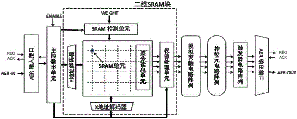
[0027] Such as figure 1 As shown, the chip of the present invention has an open-loop network structure, and the closed-loop of the chip itself, the connection between chips and the configuration of the chip by the off-chip system are flexibly realized through the AER input and output interfaces.

[0028] AER input interface includes req, ack pin and 16-bit address bus AER-IN, AER output interface includes req, ack pin, 9-bit address line AER-OUT and 1 additional configurable address. The input 16-bit bus consists of 8-bit X address, 7-bit Y address, and 1 broadcast address, and the output 9-bit bus is 8-bit X address (consisting of 7-bit output neuron address and 1 additional address) and 1 bit broadcast address.

[0029] When the corresponding req and ack between the AER input interface and output interface are respectively connect...


PUM


Abstract

The invention discloses a digital-analog hybrid neural network chip architecture. The architecture comprises a two-dimensional SRAM module, an analog synaptic circuit, a nerve cell circuit, an AER communication module, and a master control digital unit. The two-dimensional SRAM module is taken as a storage unit of neural network connection relation and a synaptic weight value. The analog synaptic circuit and the nerve cell circuit respectively consist of an MOSFET circuit working in a subthreshold section. The AER communication module serves as the input and output interfaces of a chip, and employs an AER protocol for communication. All control circuits in the architecture are synchronous digital circuits. The architecture is low in power consumption, is high in degree of parallelism, and can achieve a neural network algorithm in a reasonable chip area, wherein the neural network algorithm is more complex in nerve cell functions, is larger in network scale, and is more flexible in connection.

Description

technical field [0001] The invention relates to a chip architecture, in particular to a digital-analog hybrid neural network chip architecture, which can be used for low-power hardware implementation of neural network algorithms. Background technique [0002] The artificial neural network is a complex network system formed by extensive interconnection of a large number of simple components. It is characterized by distributed storage, asynchronous parallel processing, self-adaptation, self-learning and fault tolerance, which makes it useful in pattern recognition, speech analysis and synthesis. , computer vision and other sensory signal processing has great application prospects. However, the implementation of neural network algorithms needs to consume a lot of computing resources, especially large-scale algorithms, which usually need to resort to GPU or FPGA. [0003] Today, silicon-based VLSI technology is very mature, and research on dedicated neural network chips using C...

Claims


Application Information

Patent Timeline
Patent Type & Authority Applications(China)
IPC IPC(8): G06N3/063
CPCG06N3/065
Inventor 朱晓雷应曌中罗冲王昭王喆鸿余好雨
Owner ZHEJIANG UNIV
Why Eureka
Try Eureka