GaN-based light emitting diode epitaxial structure

A technology of light-emitting diodes and epitaxial structures, which is applied in the direction of electrical components, circuits, semiconductor devices, etc., can solve the problems of reducing the conduction band step, increasing hole injection blocking, weakening electron blocking, etc., to improve radiation recombination efficiency, The effect of reducing leakage

Inactive Publication Date: 2016-10-05
LATTICE POWER CHANGZHOU
View PDF0 Cites 18 Cited by
  • Summary
  • Abstract
  • Description
  • Claims
  • Application Information

AI Technical Summary

Problems solved by technology

However, due to the strong polarization effect in the GaN material system, the polarization electric field between the p-type AlGaN electron blocking layer and the quantum barrier will reduce the conduction band at the interface between the quantum barrier and the electron blocking layer, and weaken the electron blocking effect.
On the other hand, the p-type AlGaN electron blocking layer also has a certain resistance to the inj

Method used


Image

  • GaN-based light emitting diode epitaxial structure
  • GaN-based light emitting diode epitaxial structure
  • GaN-based light emitting diode epitaxial structure

Examples


Embodiment 1

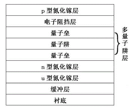
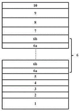
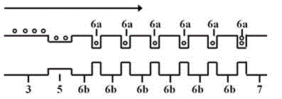
[0026] Schematic diagram of the epitaxial structure of the GaN-based LED in this embodiment, as shown in figure 2 As shown, including silicon substrate 1; AlN / Al 0.5 Ga 0.5 N / Al 0.2 Ga 0.8 N / Al 0.05 Ga 0.95 Stress control layer 2 of N four-layer structure; n-type GaN layer 3, wherein n-type GaN layer 3 includes a layer of 500nm unintentionally doped GaN layer and a layer of 3mm silicon-doped n-GaN layer, n- The doping concentration of GaN is 8×10 18 cm -3 ; n-type doped Al 0.1 Ga 0.9 N current spreading layer 4, wherein the thickness of the current spreading layer 4 is 60nm, and the doping concentration is 5×10 18 cm -3 ; Silicon doping concentration is 2×10 17 cm -3 , a thickness of 50 nm of In 0.02 Ga 0.98 N stress buffer layer 5; multi-quantum well active layer 6, whose alternating period is 6 narrow bandgap In 0.15 Ga 0.85GaN quantum barrier 6b of N quantum well 6a and wide bandgap, the thickness of quantum well / barrier is respectively 3nm / 12nm; Spacer la...

Embodiment 2

[0031] Schematic diagram of the epitaxial structure of the GaN-based LED in this embodiment, as shown in figure 2 As shown, it includes a sapphire substrate 1; the stress control layer 2 is an undoped GaN layer; the thickness of the n-type GaN layer 3 is 3um, and the doping concentration is 2×10 19 cm -3 ; The current spreading layer 4 is an alternately deposited AlGaN / InGaN superlattice structure, and an Al with a thickness of 10 nm is deposited at intervals on the n-type GaN layer 3 0.05 Ga 0.95 N layer 4b and In with a thickness of 5 nm 0.05 Ga 0.95 N layer 4a, such as Figure 5 shown, where Al 0.05 Ga 0.95 N doping concentration is 1×10 19 cm -3 , In 0.05 Ga 0.95 No doping in N; the stress buffer layer 5 is an alternately grown undoped InGaN / GaN (2nm / 5nm) superlattice, where the In composition in InGaN is 10%; the multi-quantum well active layer 6 is alternately grown 15 pairs of narrow bandgap In 0.15 Ga 0.85 GaN quantum barrier 6b of N quantum well 6a and w...


PUM

PropertyMeasurementUnit
Thicknessaaaaaaaaaa

Abstract

The invention provides a GaN-based light emitting diode epitaxial structure. From bottom to top, the structure successively comprises a substrate, a stress control layer, an n-type GaN layer, a stress buffer layer, a multi-quantum well active layer, an interval layer, an electron blocking layer, a p-type GaN layer and an ohmic contact layer. The light emitting diode epitaxial structure also comprises a current extension layer whose forbidden bandwidth is greater than the forbidden bandwidth of the n-type GaN and which is arranged below the multi-quantum well active layer. By using the epitaxial structure, electronic leakage in an active region when a light emitting diode works under a heavy current condition can be effectively reduced, radiation recombination efficiency of a hole-electron pair can be effectively increased and an antistatic characteristic of a LED is improved.

Description

technical field [0001] The invention relates to the technical field of semiconductors, in particular to an epitaxial structure of a gallium nitride-based light-emitting diode. Background technique [0002] LED (Light Emitting Diode, Light Emitting Diode) is a solid-state semiconductor device that can convert electrical energy into visible light, and it can directly convert electrical energy into light energy. LED is widely used as a new lighting source material. As a new type of light source, white LEDs are rapidly developing due to their advantages such as fast response, good shock resistance, long life, energy saving and environmental protection. Has been widely used in landscaping and indoor and outdoor lighting and other fields. [0003] The growth of the epitaxial structure is the key technology of the LED chip, and the multi-quantum well is the most important part of the epitaxial layer. For high-power GaN-based LEDs, electron leakage is an important reason for the d...

Claims


Application Information

Patent Timeline
IPC IPC(8): H01L33/04H01L33/14
Inventor 孙钱李增成黄应南孙秀建鲁德刘小平
Owner LATTICE POWER CHANGZHOU
Why Eureka
Try Eureka