Hole current shunting type power transistor with high avalanche tolerance and preparation method thereof

A power transistor and avalanche tolerance technology, which is applied in semiconductor/solid-state device manufacturing, circuits, electrical components, etc., can solve the problems of increased base resistance of parasitic triodes, increased device manufacturing costs, and low device avalanche tolerance of parasitic triodes. Achieve the effects of small leakage current, increased doping concentration, and low on-resistance

Inactive Publication Date: 2016-10-12
SOUTHEAST UNIV
View PDF5 Cites 7 Cited by
  • Summary
  • Abstract
  • Description
  • Claims
  • Application Information

AI Technical Summary

Problems solved by technology

One of the main factors causing the low avalanche tolerance of the device is that the parasitic triode is turned on prematurely. The reason why the parasitic triode is turned on prematurely is because the device is in the state of avalanche breakdown and must withstand high voltage and large current, the power of the device is large, and the temperature rises rapidly , causing the base resistance of the parasitic triode to increase rapidly, at this time a large amount of avalanche current flows through the base resistance of the parasitic triode, the base-emitter potential difference increases rapidly, and finally the parasitic triode turns on prematurely
[0004] In order to suppress the opening of the parasitic triode and improve the avalanche tolerance of the device, the current common practice is to reduce the density of the avalanche current by increasing the area of ​​the device, but the manufacturing cost of the device increases; or change the area related to the avalanche tolerance in the device The doping concentration can reduce the base resistance of the parasitic transistor, which can theoretically improve the avalanche resistance, but the effect is not obvious; or increase the depth of the contact hole to reduce the base resistance of the parasitic transistor, but the effect is also not obvious

Method used


Image

  • Hole current shunting type power transistor with high avalanche tolerance and preparation method thereof
  • Hole current shunting type power transistor with high avalanche tolerance and preparation method thereof
  • Hole current shunting type power transistor with high avalanche tolerance and preparation method thereof

Examples


Embodiment 1

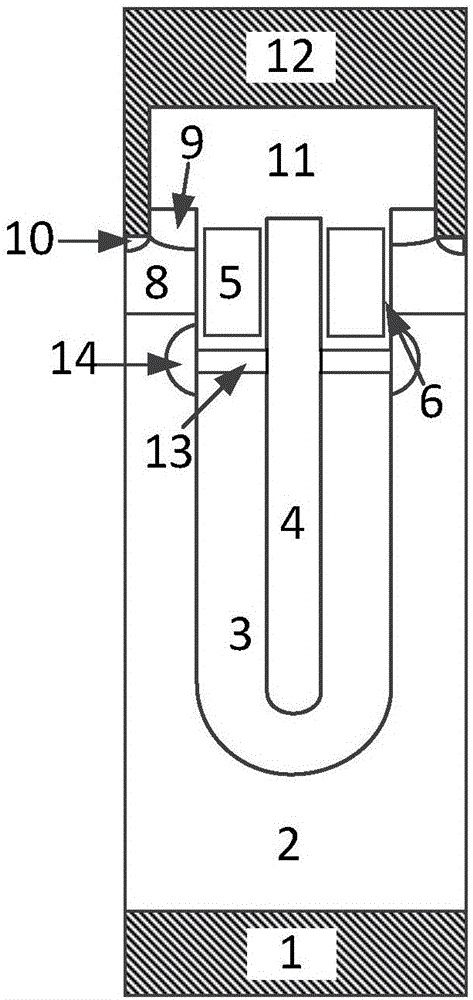
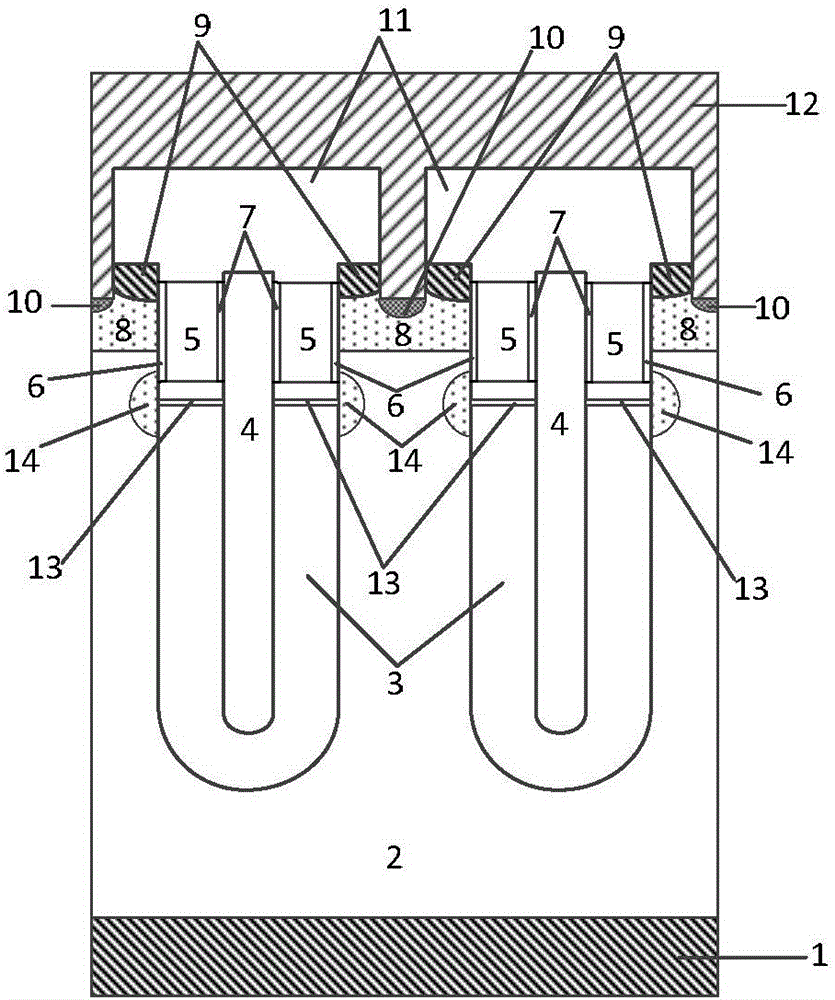
[0039] A hole current shunting power transistor with high avalanche tolerance, comprising: an N-type doped silicon substrate 1 also serving as a drain region, and an N-type doped silicon epitaxial layer 2 is arranged on the N-type doped silicon substrate 1 A trench is provided on the N-type doped silicon epitaxial layer 2, a field oxygen layer 3 is provided in the trench, a shield gate 4 and a gate 5 formed of polysilicon are provided in the field oxygen layer 3, and the gate 5 is located on both sides of the shield gate 4 and on the top of the field oxide layer 3, an insulating dielectric layer 7 is provided between the gate 5 and the shield gate 4, and at the same time, a gate oxide layer is provided between the gate 5 and the epitaxial layer 2 Layer 6, the surface of the epitaxial layer 2 between two adjacent trenches is provided with a P-type body region 8, and a P-type source region 10 and a heavily doped N-type source region 9 are arranged in the P-type body region 8 and ...

Embodiment 2

[0042] The present invention will be further described below in conjunction with specific drawings.

[0043] A preparation method of a hole current shunt power transistor with high avalanche tolerance is as follows:

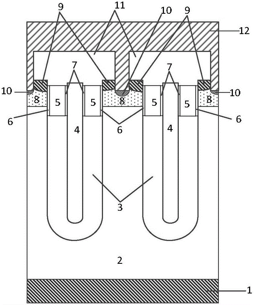
[0044] Step 1: first select an N-type silicon material as an N-type doped silicon substrate 1 and epitaxially grow an N-type doped silicon epitaxial layer 2, and then etch a groove on the N-type doped silicon epitaxial layer 2, And grow out the field oxygen layer 3, forming Figure 10A structure shown;

[0045] The second step: depositing P-type polysilicon, the concentration range of the P-type impurities is 1e14 / cm3 to 1e20 / cm3, and then etching the P-type polysilicon to form the shield gate 4, forming Figure 10B structure shown;

[0046] The third step: etching part of the field oxygen layer 3 to form Figure 10C structure shown;

[0047] Step 4: Deposit P-type polysilicon, the concentration range of P-type impurities is 0 / cm3 to 1e20 / cm3, and the curren...


PUM


Abstract

A hole-current shunt power transistor with high avalanche tolerance and a preparation method thereof, comprising: an N-type doped silicon epitaxial layer is arranged on an N-type doped silicon substrate serving as a drain region, and an N-type doped silicon epitaxial layer is provided. Grooves are arranged on the surface, and a field oxygen layer is arranged in the groove, and a shielding gate and a gate are arranged in the field oxygen layer. The gate is located on both sides of the shielding gate and on the top of the field oxygen layer. An insulating dielectric layer is provided between them, and at the same time, a gate oxide layer is provided between the gate and the epitaxial layer, a P-type body region is provided on the surface of the epitaxial layer, and a P-type source region and an N-type body region are provided on the surface of the P-type body region. The source area, the surface of the device is covered with an insulating dielectric layer, the source metal is in contact with the heavily doped N-type source area and the heavily doped P-type source area through the through hole on the insulating dielectric layer, the shielding gate is also in contact with the source metal, and the oxygen in the field A P-type polysilicon conduction channel located under the gate is arranged in the layer, one end of the P-type polysilicon conduction channel is connected to the N-type doped silicon epitaxial layer, and the other end is connected to the shielding grid.

Description

technical field [0001] The invention belongs to the technical field of semiconductor power devices, and relates to a power semiconductor transistor with high avalanche tolerance and a preparation method thereof, and is especially suitable for electric vehicles, motor speed regulation, inverters, uninterruptible power supplies, electronic switches, high-fidelity audio, and automobiles. Electrical and electronic rectifiers. Background technique [0002] As a deep trench metal oxide semiconductor field effect transistor, the shielded gate field effect transistor has a small on-resistance, and has a smaller Miller capacitance than the traditional deep trench metal oxide semiconductor field effect transistor, so Its switching speed is significantly improved, and the turn-off loss is significantly reduced. Therefore, shielded gate field effect transistors are widely used, and can be applied to motor speed regulation, inverters, uninterruptible power supplies, electronic switches, ...

Claims


Application Information

Patent Timeline
Patent Type & Authority Applications(China)
IPC IPC(8): H01L29/78H01L29/06H01L21/336
CPCH01L29/78H01L29/0688H01L29/66409
Inventor 祝靖周锦程杨卓宋慧滨孙伟锋陆生礼时龙兴
Owner SOUTHEAST UNIV
Why Eureka
Try Eureka