LED epitaxial wafer growing on yttrium aluminum garnet substrate and manufacturing method
A technology of LED epitaxial wafer and yttrium aluminum garnet, which is applied in the field of LED epitaxial wafer and preparation, can solve the problems of affecting the performance of GaN-based devices, reducing the carrier mobility of materials, reducing the internal quantum efficiency of the device, etc., so as to improve the internal quantum efficiency. Efficiency, improved radiation recombination efficiency, small lattice mismatch
- Summary
- Abstract
- Description
- Claims
- Application Information
AI Technical Summary
Problems solved by technology
Method used
Image
Examples
Embodiment 1
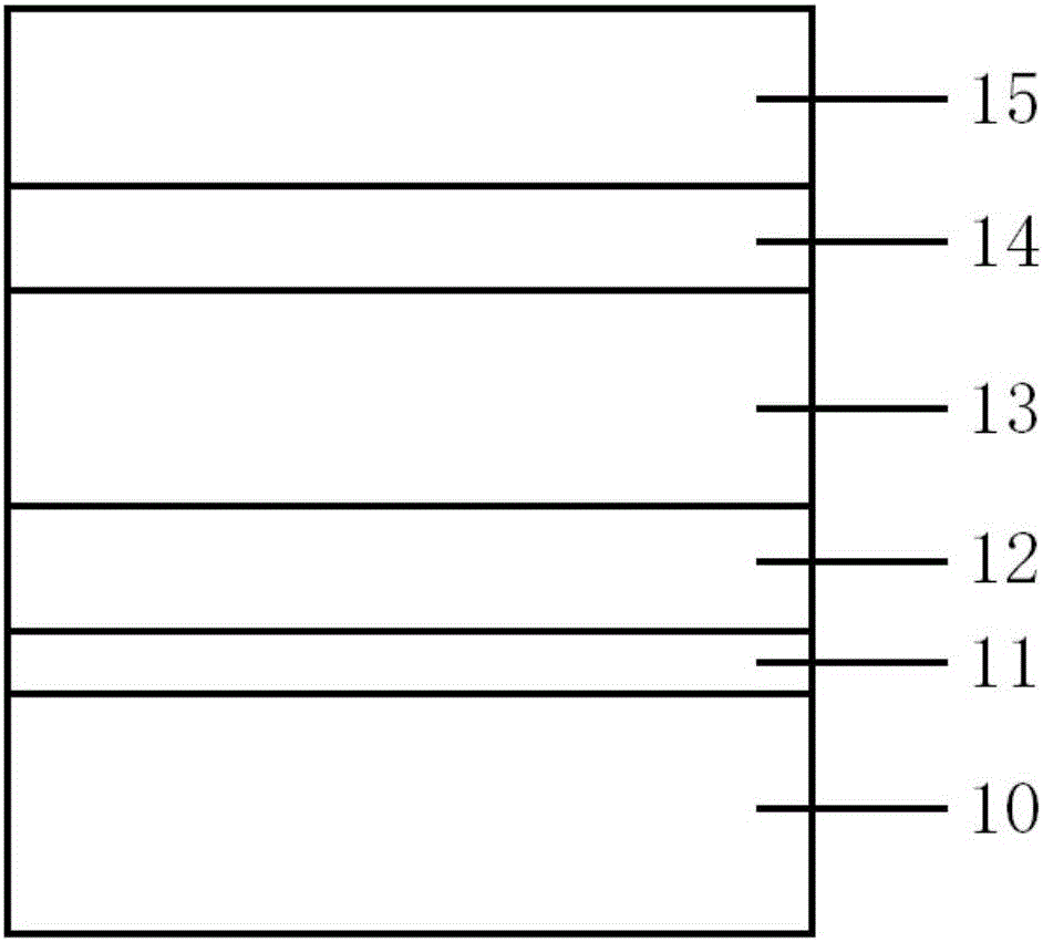
[0037] A kind of LED epitaxial wafer grown on the yttrium aluminum garnet substrate, its preparation method comprises the following steps:
[0038] (1) Selection of the substrate and its crystal orientation: Y 3 al 5 o 12 The substrate, with the (111) plane offset from the (100) plane by 0.5° as the epitaxial plane, the crystal epitaxial orientation relationship is: the (0001) plane of GaN is parallel to the Y 3 al 5 o 12 (111) side;
[0039] (2)Y 3 al 5 o 12 Substrate surface annealing treatment, the specific process is: Y 3 al 5 o 12 The substrate was placed in the reaction chamber, and the Y 3 al 5 o 12 The substrate is annealed in situ for 2 hours, and the annealing treatment can make Y 3 al 5 o 12 The substrate obtains an atomically flat surface;
[0040] (3) Epitaxial growth of GaN buffer layer: Y 3 al 5 o 12 The substrate temperature was adjusted to 400°C, and the pressure in the reaction chamber was 4.0×10 -3 A GaN buffer layer with a thickness of ...
Embodiment 2
[0049] A kind of LED epitaxial wafer grown on the yttrium aluminum garnet substrate, its preparation method comprises the following steps:
[0050] (1) Selection of the substrate and its crystal orientation: Y 3 al 5 o 12 The substrate, with the (111) plane offset from the (100) plane by 1° as the epitaxial plane, the crystal epitaxial orientation relationship is: the (0001) plane of GaN is parallel to the Y 3 al 5 o 12 (111) side;
[0051] (2)Y 3 al 5 o 12 Substrate surface annealing treatment, the specific process is: Y 3 al 5 o 12 The substrate was placed in the reaction chamber, and the Y 3 al 5 o 12 The substrate is subjected to in-situ annealing treatment for 1 hour, and the annealing treatment can make the substrate obtain an atomically flat surface;
[0052] (3) Epitaxial growth of GaN buffer layer: Y 3 al 5 o 12 The substrate temperature was adjusted to 500°C, and the pressure in the reaction chamber was 6.0×10 -3 A GaN buffer layer with a thickness ...
PUM
| Property | Measurement | Unit |
|---|---|---|
| thickness | aaaaa | aaaaa |
| thickness | aaaaa | aaaaa |
| thickness | aaaaa | aaaaa |
Abstract
Description
Claims
Application Information
 - R&D
- Intellectual Property
- Life Sciences
- Materials
- Tech Scout
- Unparalleled Data Quality
- Higher Quality Content
- 60% Fewer Hallucinations
Browse by: Latest US Patents, China's latest patents, Technical Efficacy Thesaurus, Application Domain, Technology Topic, Popular Technical Reports.
© 2025 PatSnap. All rights reserved.Legal|Privacy policy|Modern Slavery Act Transparency Statement|Sitemap|About US| Contact US: help@patsnap.com


