Two-dimensional nano molybdenum sulfide sheet layer/binary oxide laminated structure type resistive random access memory
A binary oxide and two-dimensional nanotechnology, applied in the field of microelectronics and nanomaterials, to achieve the effect of simple equipment, large size, and easy control of material components
- Summary
- Abstract
- Description
- Claims
- Application Information
AI Technical Summary
Problems solved by technology
Method used
Image
Examples
Embodiment 1
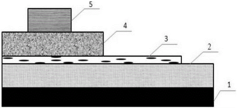
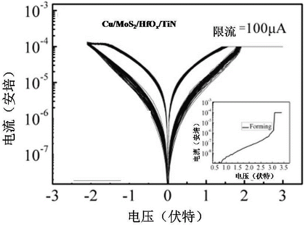
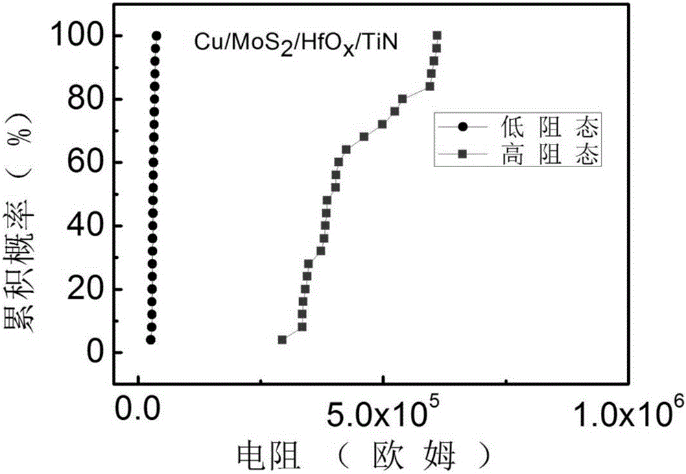
[0030] A resistive switching device with a two-dimensional nanomolybdenum sulfide sheet layer / binary oxide stack structure, such as figure 1 Shown by Si / SiO 2 The substrate 1, the lower electrode 2, the resistive switch layer and the upper electrode 5 are sequentially stacked, wherein the resistive switch layer is a laminated structure of binary oxide 3 and two-dimensional nanomolybdenum sulfide sheet layer 4, and the material of the lower electrode is 100nm Thick TiN, binary oxide is 25nm HfO 2 The thin film, the two-dimensional nano-molybdenum sulfide sheet layer is a single layer, and the bottom electrode material is Cu with a thickness of 15nm.
[0031] The preparation method of the two-dimensional nano-molybdenum sulfide sheet layer / binary oxide stack structure resistance switch device, the steps are as follows:
[0032] 1) Si / SiO 2 Deposit 100nm TiN as the bottom electrode by magnetron sputtering for the substrate;
[0033] 2) Uniformly coat a layer of photoresist on...
Embodiment 2
[0042] A two-dimensional nano-molybdenum sulfide layer / binary oxide stack structure resistive switch device, the structure is basically the same as that of Example 1, the difference is that: the two-dimensional nano-molybdenum sulfide layer is multi-layered, the thickness is 5nm, prepared The method is the micromechanical exfoliation method. Its preparation and testing steps are the same as in Example 1. The number of two-dimensional nanomolybdenum sulfide sheets used is different)
Embodiment 3
[0044] A two-dimensional nano-molybdenum sulfide layer / binary oxide stack structure resistance switch device, the structure is basically the same as that of Example 1, the difference is that the binary oxide is 25nmTaO 2 film. Its preparation and testing steps are the same as in Example 1.
PUM
| Property | Measurement | Unit |
|---|---|---|
| Thickness | aaaaa | aaaaa |
Abstract
Description
Claims
Application Information
 - R&D Engineer
- R&D Manager
- IP Professional
- Industry Leading Data Capabilities
- Powerful AI technology
- Patent DNA Extraction
Browse by: Latest US Patents, China's latest patents, Technical Efficacy Thesaurus, Application Domain, Technology Topic, Popular Technical Reports.
© 2024 PatSnap. All rights reserved.Legal|Privacy policy|Modern Slavery Act Transparency Statement|Sitemap|About US| Contact US: help@patsnap.com


