

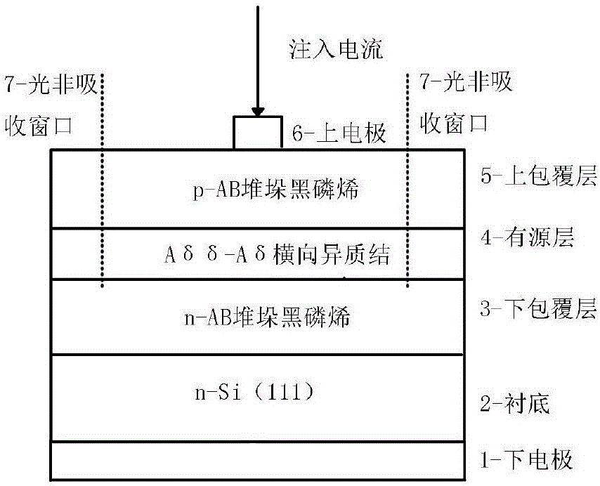
Heterojunction semiconductor laser and manufacturing method thereof
A heterojunction and semiconductor technology, applied in the direction of semiconductor lasers, lasers, laser components, etc., can solve the problems of large beam divergence angle, large temperature influence, poor directionality, monochromaticity and coherence, etc., and achieve easy lattice The effect of matching, reducing injection current, and improving conversion efficiency
- Summary
- Abstract
- Description
- Claims
- Application Information
AI Technical Summary
Problems solved by technology
Method used
Image

Examples
Embodiment Construction
[0032] a. Preparation of the substrate: using n-type silicon as the substrate;
[0033] n-Si substrate cleaning: take n-Si (111) sheet as the substrate, soak it with olefinic HF acid to remove the silicon dioxide on the Si surface, and then use propanol, ethanol, and deionized water to ultrasonically clean it to remove the silicon dioxide on the silicon sheet. Dry the organic matter with nitrogen, and put it into a quartz tube for deposition treatment; the vacuum degree of the quartz tube is about 10-2Pa, and it is heated to about 300°C for 10-15 minutes to remove the water vapor on the surface of the silicon wafer;
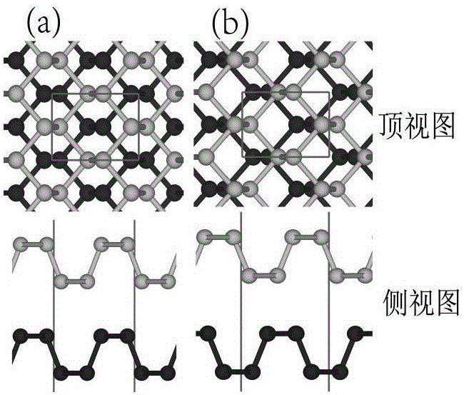
[0034] b. Preparation of few-layer black phosphorene: Bulk black phosphorus is obtained by treating its isomorph white phosphorus or red phosphorus under high temperature and high pressure:
[0035] 1) White phosphorus was heated to 200°C at 1200 atmospheres to obtain flaky black phosphorus; the multi-layer black phosphorene was peeled off from the black phosphor...
PUM
| Property | Measurement | Unit |
|---|---|---|
| Thickness | aaaaa | aaaaa |
Abstract
Description
Claims
Application Information