Preparation method for embedded multi-orientation metal nanowire transparent conductive film

A transparent conductive film, metal nanowire technology, applied in conductive materials dispersed in non-conductive inorganic materials, cable/conductor manufacturing, circuits, etc. The effect of transparency and high conductivity

Active Publication Date: 2016-10-26
SUN YAT SEN UNIV
View PDF9 Cites 16 Cited by
  • Summary
  • Abstract
  • Description
  • Claims
  • Application Information

AI Technical Summary

Problems solved by technology

However, some studies have pointed out that PE

Method used


Image

  • Preparation method for embedded multi-orientation metal nanowire transparent conductive film
  • Preparation method for embedded multi-orientation metal nanowire transparent conductive film
  • Preparation method for embedded multi-orientation metal nanowire transparent conductive film

Examples


Example Embodiment

[0034] Example 1 Temporary substrate hydroxylation

[0035] In this case, the temporary substrate is processed by hydroxylation to increase the hydrophilicity of the substrate surface, which is conducive to the uniform distribution of the metal nanowires on the substrate surface and the formation of oriented arrangement. In addition, hydroxyl groups provide reaction sites for subsequent grafting of anti-adhesive groups; the temporary substrate used can be a flexible substrate or a rigid substrate; the hydroxylation treatment used can be surface grafting with chemical solutions or ultraviolet ozone treatment, etc. . Two examples are given below for description:

[0036] If the temporary substrate used is flexible polyethylene terephthalate (PET). It was immersed in the APTES-toluene mixed solution by pulling and dipping, the APTES concentration was 5wt%, the immersion time was 10min, and then it was pulled out from APTES at a speed of 2000μm / s. The contact angle of the obtained P...

Example Embodiment

[0038] Example 2 Preparation of dual-oriented nano silver wire transparent film

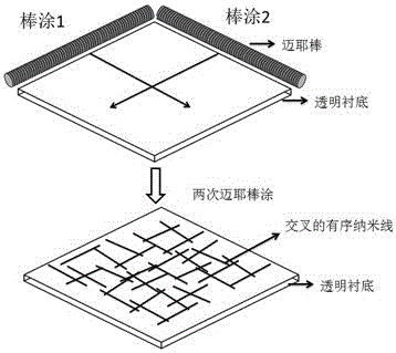
[0039] For one-dimensional metal nanowires, the micro-textures on the Meyer rod are used to guide the nanowires during the rod coating process to control the orientation of the nanowires. After a single coating, the film is dried, and then the next nanowire orderly coating is performed to obtain dual-oriented ordered metal nanowires to form a uniform conductive network.

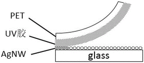
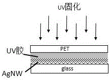
[0040] In this case, hydroxylated glass was used as a temporary substrate, and silver nanowires were used as metal nanowires to prepare multilayer ordered conductive films. The silver nanowires used have an average diameter of 34 nm and a length of 18 μm. The silver nanowires are dispersed in an ethanol solution with a concentration of 10 mg / ml. The nano silver wire dispersion is mixed with anhydrous isopropanol in a mass ratio of 1:4, and then shaken evenly after sonicating for 2 minutes.

[0041] In this case, a Meyer rod with a wi...

Example Embodiment

[0043] Example 3 Selective Hydrophilic Treatment

[0044] The key step of the present invention is to selectively modify the nano silver wire-temporary substrate, that is, only the modified substrate is hydrophobically modified, and the nano silver wire itself is not modified.

[0045] Preferably, hexamethyldisilane is used as the modification material. Pipette 2 ml of hexamethyldisilane solution, drop it into a petri dish, and place it in a closed oven with a temperature of 70°C; place the above-mentioned ordered silver nanowire-hydroxylated glass on top of the solution.

[0046] During the evaporation of the solution, the imino groups of the hexamethyldisilane solution react with the hydroxyl groups on the glass surface to produce trimethylsiloxy groups. In order to fully react, the deposition time is set to 20 minutes. Pure silver nanowires have no hydroxyl groups, so they will not bond with silane and their surface will not be hydrophobized. The purpose of this step is to redu...


PUM

PropertyMeasurementUnit
The average diameteraaaaaaaaaa
Lengthaaaaaaaaaa

Abstract

The invention discloses a preparation method for an embedded multi-orientation metal nanowire transparent conductive film. The preparation method comprises the following steps that S1. a metal nanowire solution is added in a temporary substrate and then metal nanowires are arranged in an orientation way, wherein the temporary substrate is made of hydrophilic material; S2. surface modification is performed on the temporary substrate so that the temporary substrate is enabled to be hydrophobic from being hydrophilic, and a surface modified substrate-metal nanowire film is obtained; and S3. embedding and stripping process is performed: the metal nanowires are embedded in cure adhesive by using the cure adhesive and the cure adhesive is stripped from the temporary substrate. The hydrophilic and hydrophobic performance of the temporary substrate is adjusted so that the embedded multi-orientation metal nanowire transparent conductive film having better conductivity, adhesiveness, flatness and stability is obtained.

Description

technical field [0001] The invention relates to the field of film conduction, in particular to a method for preparing an embedded multi-orientation metal nanowire transparent conductive film. Background technique [0002] Transparent conductive film is a basic optoelectronic material with high conductivity and high transparency in the visible light band. It is widely used in optoelectronic display fields such as displays, light-emitting devices, solar cells, sensors, and flexible touch screens. It has broad commercial application prospects. The traditional transparent conductive film is based on indium tin oxide material. Although the display optoelectronic manufacturing technology based on this material is quite mature, the cost is relatively high because indium tin oxide contains rare materials; and the flexibility of indium tin oxide film is very poor. , cannot be used to prepare flexible displays, and is greatly limited in application. In recent years, scientists have d...

Claims


Application Information

Patent Timeline
IPC IPC(8): H01B13/00H01B1/22
CPCH01B1/22H01B13/0013
Inventor 杨柏儒刘贵师许钰旺陈鹏谢汉萍
Owner SUN YAT SEN UNIV
Why Eureka
Try Eureka