Manufacturing method of back surface polishing crystalline silicon solar battery

A technology for solar cells and manufacturing methods, applied in the direction of final product manufacturing, sustainable manufacturing/processing, circuits, etc., can solve the problems of corrosion of the N-type diffusion layer of the solar cell, damage to the PN junction of the solar cell, and reduction of the conversion efficiency of the solar cell. , to achieve the effect of improving uniformity, avoiding damage, and improving photoelectric conversion efficiency

Inactive Publication Date: 2016-10-26
JIANGXI UNIV OF TECH
View PDF7 Cites 1 Cited by
  • Summary
  • Abstract
  • Description
  • Claims
  • Application Information

AI Technical Summary

Problems solved by technology

[0003] As mentioned above, the acid solution used in the back surface polishing process will volatilize to form acid mist, which will corrode the N-type diffusion layer of the solar cell, thereby destroying the PN junction of the solar cell and reducing the conversion efficiency of the solar cell

Method used


Image

  • Manufacturing method of back surface polishing crystalline silicon solar battery
  • Manufacturing method of back surface polishing crystalline silicon solar battery
  • Manufacturing method of back surface polishing crystalline silicon solar battery

Examples


Embodiment Construction

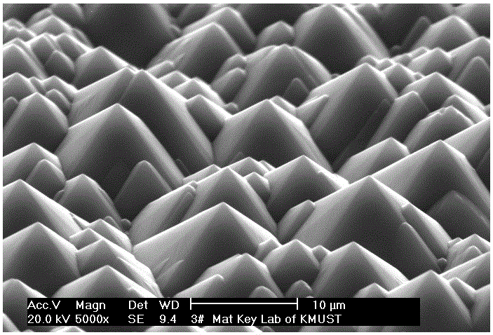
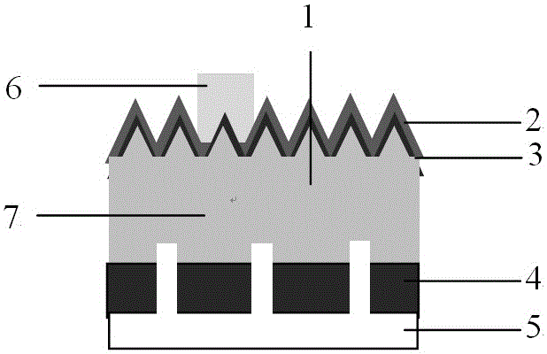
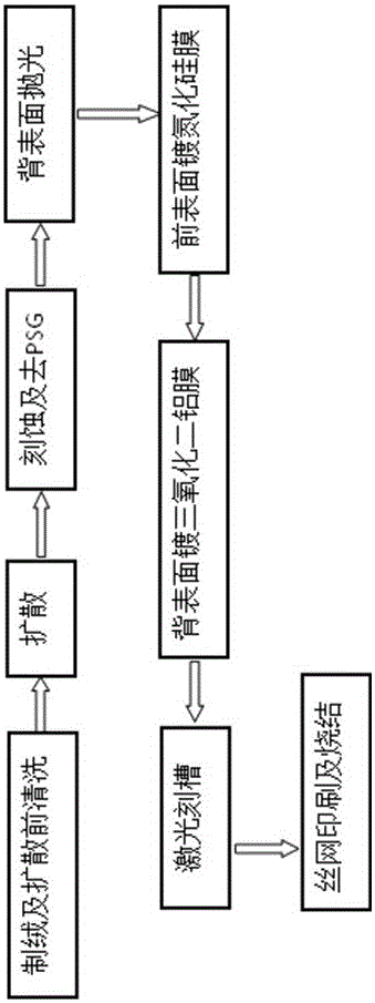
[0019] The specific embodiments of the present invention are described by taking the manufacturing of a back surface polished local point contact crystalline silicon solar cell as an example.

[0020] The manufacturing process of the back surface polishing local point contact crystalline silicon solar cell is as follows Figure 4 As shown, it includes: back surface coating, texturing and cleaning before diffusion, diffusion, wet etching and PSG removal, silicon nitride film coating on the front surface, aluminum oxide film coating on the back surface, laser Grooving, screen printing and sintering. The following is a detailed description of each process, the specific content is as follows:

[0021] 1. Coating on the back surface

[0022] Use as Figure 5 (A) The ordinary P-type silicon wafer as shown. The main purpose of the back surface coating process is to plate a layer of mask 8 on the back surface of the P-type silicon wafer as a protective layer on the back surface, such as ...


PUM


Abstract

The invention discloses a manufacturing method of a back surface polishing crystalline silicon solar battery. The method comprises the following concrete steps: performing texturing and cleaning before diffusion; performing the diffusion; performing wet etching and PSG removal; plating a front surface with a silicon nitride film; plating a back surface with an alundum (Al2O3) membrane; performing laser groove etching; and performing screen printing and sintering. The method is characterized in that before the texturing and the cleaning before the diffusion, a back surface membrane plating process is also arranged, i.e., the back surface of an initial P-type silicon chip is plated with the silicon nitride film with a mask effect according to a conventional method. Compared to a conventional process, the method has the following advantages: only the back surface membrane plating process is added before a texturing and pre-diffusion cleaning process begins, at the same time, an individual back surface polishing process of the P-type silicon chip is omitted, back-surface polishing of the P-type silicon chip can also be realized, damage caused by the individual back surface polishing process to a solar battery N-type diffusion layer is avoided, and therefore, the photoelectric conversion efficiency of the crystalline silicon solar battery can be improved.

Description

Technical field [0001] The invention relates to the manufacturing field of crystalline silicon solar cells, and in particular to a method for manufacturing a back surface polished crystalline silicon solar cell. Background technique [0002] Surface polishing can improve the uniformity of the back surface field, and is particularly beneficial to the realization of the local point contact process on the back surface. The texturing process in the crystalline silicon solar cell manufacturing process will cause the back surface of the cell to form such as figure 1 The suede structure shown, due to the presence of suede on the back surface, makes the wet etching and PSG removal process unable to polish the back surface. In this way, it is necessary to add a separate back surface polishing process after the wet etching and PSG removal process to realize the back surface polishing of the solar cell. Such as image 3 As shown, the normal back surface polishing local point-contact crysta...

Claims


Application Information

Patent Timeline
Patent Type & Authority Applications(China)
IPC IPC(8): H01L31/18
CPCH01L31/18Y02P70/50
Inventor 王国宁周青曾玉
Owner JIANGXI UNIV OF TECH
Why Eureka
Try Eureka