

Method for preparing high-quality perovskite crystal thin film
A perovskite, high-quality technology, applied in the direction of electrical solid devices, semiconductor devices, semiconductor/solid device manufacturing, etc., can solve the problems of difficult to completely convert perovskite, perovskite layer dissolution, PbI residue, etc., to shorten the preparation time Period, uniform grain size distribution, and good crystallinity
- Summary
- Abstract
- Description
- Claims
- Application Information
AI Technical Summary
Problems solved by technology
Method used
Image

Examples
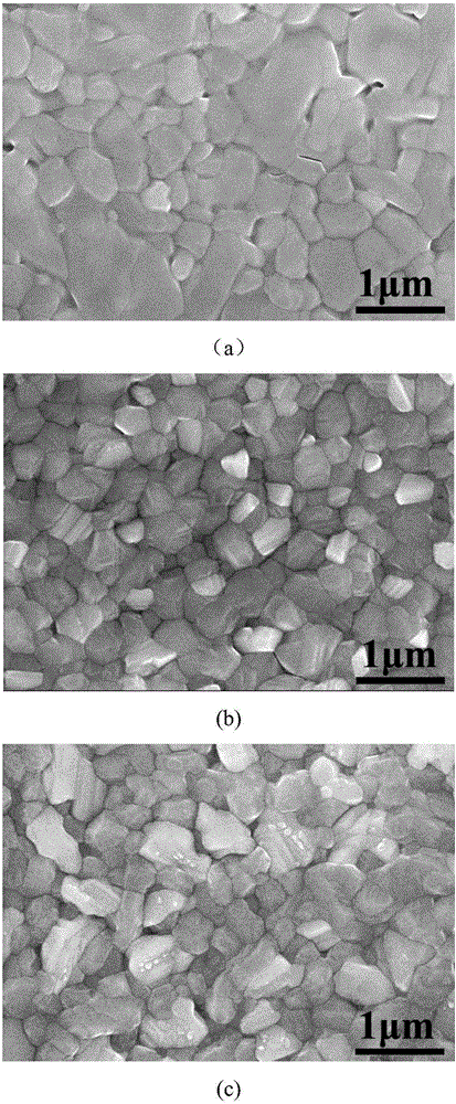
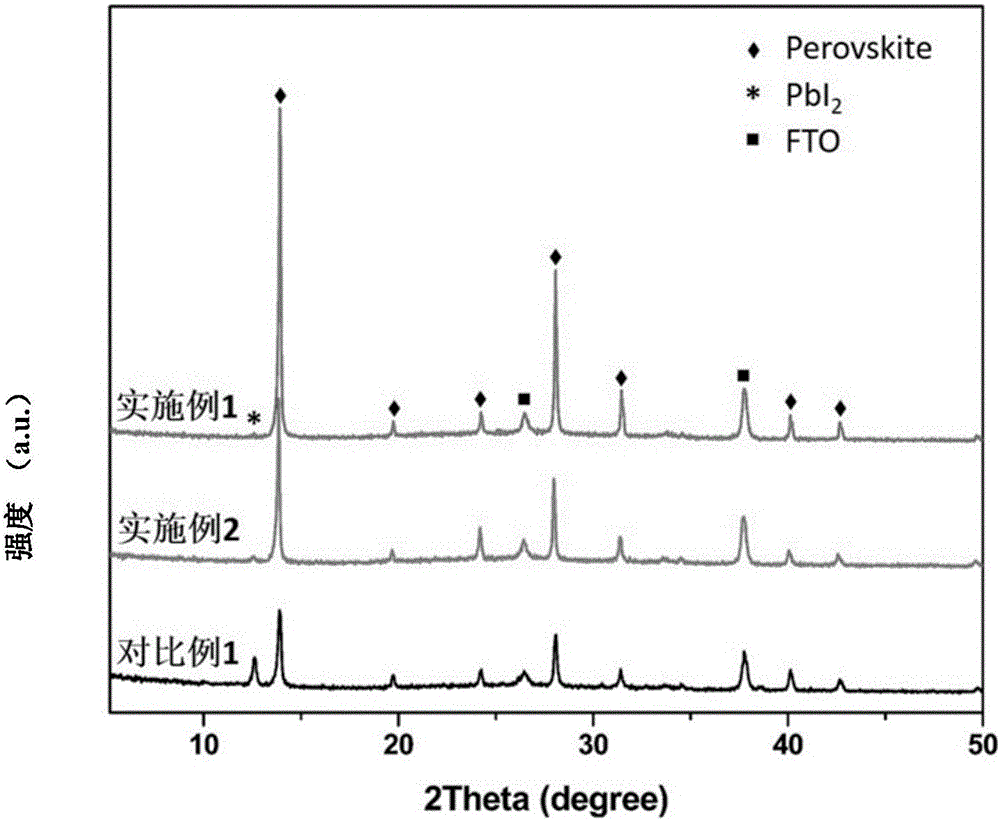
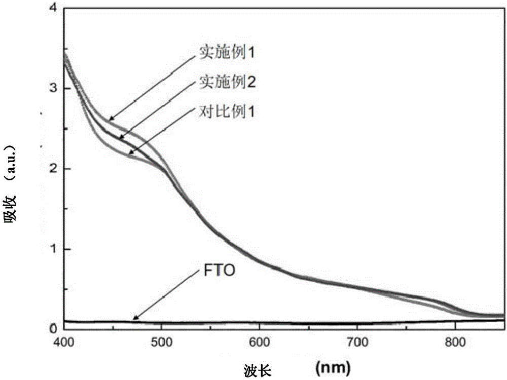
Embodiment 1
[0041] (1) Preparation of reaction solution
[0042] PbI 2 and DMSO were added to the DMF solvent, where PbI 2 The concentration is 1M, DMSO and PbI 2 Equivalent molar ratio, then magnetically stirred at room temperature for 1 hour to make PbI 2 Completely dissolve to obtain reaction solution A; mix methylammonium iodide (MAI) and formamidinium iodide (FAI) in a molar ratio of 1:9, and then dissolve the mixture in isopropanol solvent In , the concentration of the solute in the mixture was 0.41 mM, and the solute was completely dissolved by shaking to obtain the reaction solution B.
[0043] (2) Spin coating film formation
[0044] a) Dense TiO2 layer and mesoporous TiO have been formed on the heated surface 2 Layer the FTO conductive substrate so that its temperature is maintained at 65 °C.
[0045] b) The reaction solution A prepared in step (1) is added dropwise on the substrate prepared in a) above, and spin-coated for the first time to form PbI 2 film, wherein the r...
Embodiment 2
[0050] (1) Preparation of reaction solution
[0051] PbI 2 and DMSO were added to the DMF solvent, where PbI 2 The concentration is 1M, DMSO and PbI 2 Equivalent molar ratio, then magnetically stirred at room temperature for 1 hour to make PbI 2 Completely dissolve to obtain reaction solution A; mix MAI and FAI at a molar ratio of 3:7, then dissolve the mixture in isopropanol solvent, the solute concentration of the mixture is 0.41mM, shake to completely dissolve the solute to obtain reaction solution B.
[0052] (2) Spin coating film formation
[0053] Same as step (2) in Example 1.
[0054] (3) heat treatment
[0055] Same as step (3) in Example 1.
Embodiment 3
[0057] (1) Preparation of reaction solution
[0058] PbI 2 and DMSO were added to the DMF solvent, where PbI 2 The concentration is 0.8M, DMSO and PbI 2 Equivalent molar ratio, then magnetically stirred at room temperature for 1 hour to make PbI 2 Completely dissolve to obtain reaction solution A; mix MAI and FAI at a molar ratio of 9:1, then dissolve the mixture in isopropanol solvent, the solute concentration of the mixture is 0.43mM, shake to completely dissolve the solute to obtain reaction solution B.
[0059] (2) Spin coating film formation
[0060] a) Dense TiO has been formed on the heated surface 2 layer and mesoporous TiO 2 Layer the FTO conductive substrate so that its temperature is maintained at 65 °C.
[0061] b) Add the reaction solution A prepared in step (1) dropwise to the mesoporous TiO formed in a) above 2 layer, the first spin coating is performed to form a PbI 2 film, wherein the rotation speed is 3500rpm, the spin coating time is 30s, and the amo...
PUM
 Abstract
Description
Claims
Application Information