Preparation method of AlN film based on patterned sapphire substrate (PPS)

A thin film and sputtering coating technology, applied in ion implantation plating, metal material coating process, coating and other directions, can solve the problems of large warpage and high production cost in epitaxial growth, save process time and reduce defect density , The effect of improving yield and output power

Inactive Publication Date: 2016-11-09
ZHEJIANG EAST CRYSTAL BOLANTE PHOTOELECTRIC
View PDF2 Cites 7 Cited by
  • Summary
  • Abstract
  • Description
  • Claims
  • Application Information

AI Technical Summary

Problems solved by technology

[0005] The purpose of the present invention is to provide a new and practical method for preparing PSS-based AlN thin films to produce PSS substrates with large bottom widths and to solve the problems of excessive warpage and high production costs in the production process of existing LED devices. bottom, improve the yield of LED chips

Method used


Image

  • Preparation method of AlN film based on patterned sapphire substrate (PPS)
  • Preparation method of AlN film based on patterned sapphire substrate (PPS)
  • Preparation method of AlN film based on patterned sapphire substrate (PPS)

Examples


Embodiment

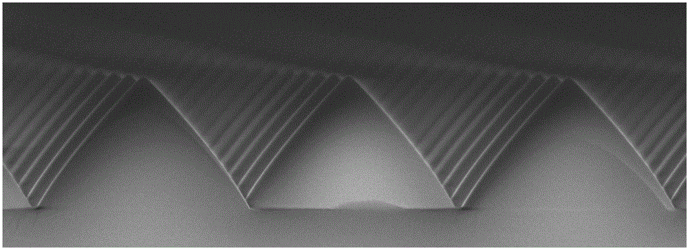
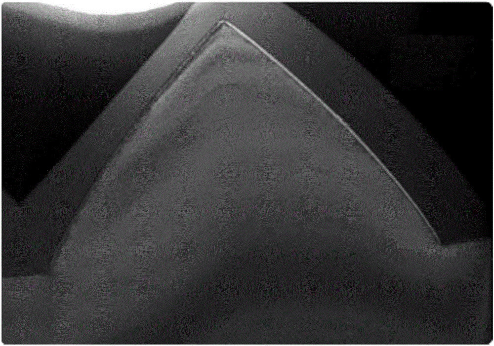
[0034] Select a piece of wafer, the wafer is Ф101.6mm×0.650mm PSS wafer, its microscopic appearance is as follows figure 1 As shown, the equipment used is a sputtering coating machine, and the workshop meets the requirements of a class 100 clean room standard. The following specific steps are followed to prepare the PSS-based AlN film:

[0035](1) Select a piece of PSS wafer, and pre-treat the PSS wafer and the Al target, wherein the pre-treatment of the PSS wafer includes: sequentially using analytical grade isopropyl ketone and alcohol to scrub the PSS wafer to remove grease and water on the surface of the PSS wafer and other dirt, then blow it off with compressed air with a pressure of 1.2MPa, and finally place the processed PSS wafer on the anode plate, cover the vacuum cover, and keep the reaction chamber clean;

[0036] The pretreatment of the Al target includes: wipe the round Al target with a purity of 99.99% with a dust-free cloth soaked in isopropanol to remove the o...


PUM

PropertyMeasurementUnit
heightaaaaaaaaaa
thicknessaaaaaaaaaa
surface roughnessaaaaaaaaaa

Abstract

The invention discloses a preparation method of an AlN film based on a patterned sapphire substrate (PPS). The method comprises the following steps that (1) a PSS wafer is selected, and the PSS wafer and an Al target are pretreated; (2) a reaction chamber is vacuumized, and the PSS wafer is placed in the vacuumized reaction chamber; (3) the PSS wafer is cleaned with low energy, so that an oxide layer on the surface of the wafer is removed; (4) the PSS wafer is heated to be at a certain temperature through currents; (5) the PSS wafer is subjected to pre-sputtering in a vacuum environment; (6) sputter coating is carried out at a stable air pressure, and the AlN film based on the PSS is obtained; and (7) equipment is shut down, and the prepared AlN film based on the PSS is taken out. The graph dimension of the PPS is 2.6-2.8 microns, the height of the PPS is 1.6-1.8 microns, the thickness of the AlN film is 15-50 nm, the half-peak width is 160-180 arcsec, and the surface roughness is 0.3-0.5 nm. According to the method, patterned sapphire is adopted as the substrate, the AlN film is prepared through the plasma magnetron sputtering method, by means of the AlN film, the warping during epitaxial growth of the sapphire can be greatly reduced, and the yield and output power of an LED chip are greatly improved.

Description

technical field [0001] The invention relates to the technical field of LED chip sapphire substrates, in particular to a method for preparing a PSS-based AlN thin film. Background technique [0002] With the rapid development of the current solid-state high-tech industry, including integrated circuit industry, solid-state light emitting, laser device industry, magnetic recording material and device industry, etc., more and more attention has been paid to thin-film scientific research and technology, and the contribution of thin-film research and development to production Increasingly, thin-film scientific research results are being transformed into productivity faster and faster. Electronic thin film materials are the basis of microelectronic technology and optoelectronic technology, so the research on various new electronic thin film materials has become the focus of attention of scientists today. [0003] PSS (Patterned Sapphire Substrate), that is, a patterned sapphire su...

Claims


Application Information

Patent Timeline
Patent Type & Authority Applications(China)
IPC IPC(8): C23C14/35C23C14/06C23C14/02
CPCC23C14/35C23C14/0036C23C14/022C23C14/0617
Inventor 刘建哲褚君尉彭艳亮杨新鹏郑小琳陈素春徐良
Owner ZHEJIANG EAST CRYSTAL BOLANTE PHOTOELECTRIC
Why Eureka
Try Eureka