Epitaxial growth method of light-emitting diode with well region doping
A technology of light-emitting diodes and epitaxial growth, which is used in electrical components, circuits, semiconductor devices, etc. to increase the recombination efficiency, reduce the operating voltage, and reduce the luminous efficiency.
- Summary
- Abstract
- Description
- Claims
- Application Information
AI Technical Summary
Problems solved by technology
Method used
Image
Examples
Embodiment Construction
[0036] The present invention will be described in detail below in conjunction with the accompanying drawings and specific embodiments.
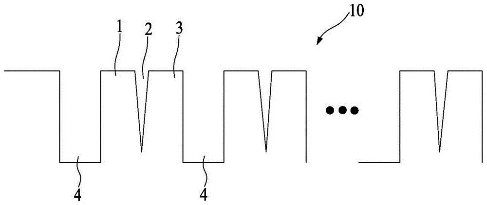
[0037] refer to figure 1 As shown, the present invention discloses a light-emitting diode with well doping, on which a buffer layer, an unintentionally doped GaN layer, an n-GaN layer, an active region, an electron blocking layer, a p- GaN layer and ohmic contact layer.
[0038] The active region 10 is composed of a front quantum barrier 1, a V-type quantum well 2, a rear quantum barrier 3 and a quantum well 4, which are periodically stacked in sequence, and the V-type quantum well 2 is doped. The V-type quantum well 2 is n-type doped, and the doping concentration is ≧1E+18. Using high-concentration doping can reduce the resistance value of the entire active region 10 , and can effectively reduce the working voltage of the light-emitting diode after being fabricated into chips. The V-type quantum well 2 is preferably doped with Si.
[0039...
PUM
| Property | Measurement | Unit |
|---|---|---|
| Thickness | aaaaa | aaaaa |
Abstract
Description
Claims
Application Information
