Semiconductor structure, semiconductor assembly and power semiconductor device

A technology of power semiconductors and semiconductors, which is applied in the direction of semiconductor devices, semiconductor/solid-state device parts, electrical components, etc., can solve the problems of small breakdown voltage and low voltage withstand capacity, and achieve improved breakdown voltage, reliability, and The effect of preventing premature breakdown

Active Publication Date: 2016-11-16
UNIV OF ELECTRONICS SCI & TECH OF CHINA +1
View PDF4 Cites 5 Cited by
  • Summary
  • Abstract
  • Description
  • Claims
  • Application Information

AI Technical Summary

Problems solved by technology

[0011] In view of the above-mentioned shortcomings of the prior art, the object of the present invention is to provide a semiconductor structure, a semiconductor component and a power semiconductor device to solve the problems of the diode structure in the prior art with low breakdown voltage and low voltage withstand capability. The problem

Method used


Image

  • Semiconductor structure, semiconductor assembly and power semiconductor device
  • Semiconductor structure, semiconductor assembly and power semiconductor device
  • Semiconductor structure, semiconductor assembly and power semiconductor device

Examples


Embodiment 1

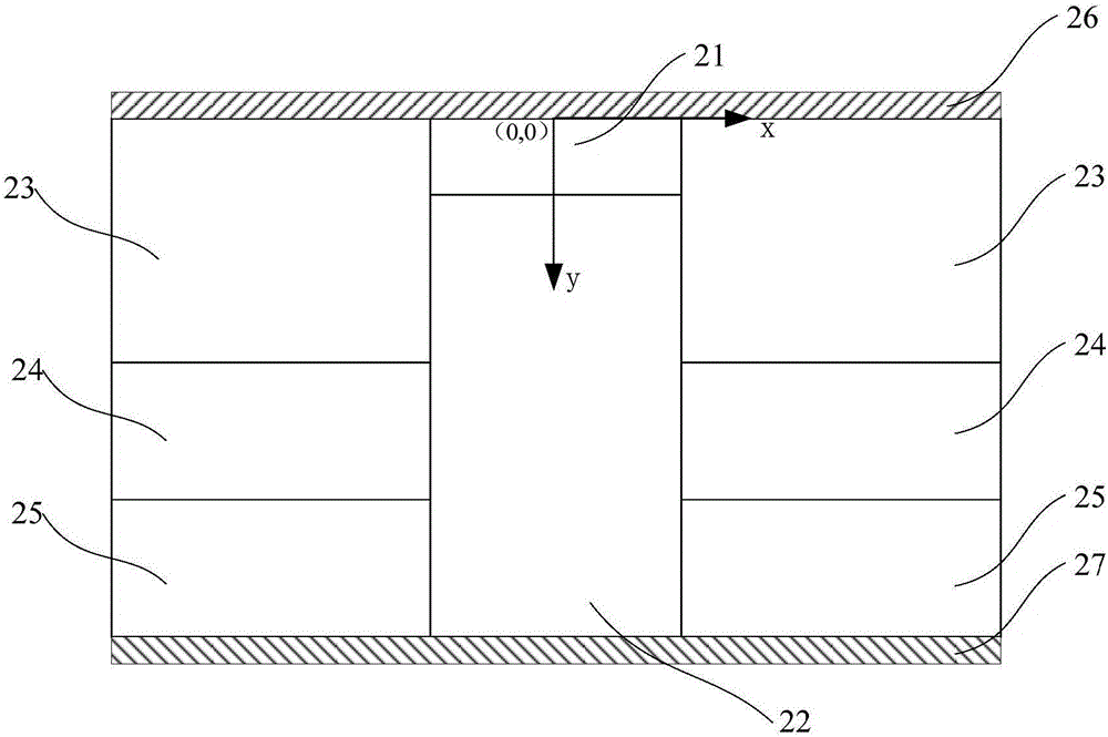
[0082] see figure 2 , the present invention provides a semiconductor structure, the semiconductor structure includes: P-type semiconductor material layer 21; N-type semiconductor material layer 22, the N-type semiconductor material layer 22 is adjacent to the P-type semiconductor material layer 21 , together with the P-type semiconductor material layer 21 to form a PN junction; a multi-layer insulating material layer, located outside the PN junction, and stacked with the N-type semiconductor material layer 22 along the P-type semiconductor material layer 21 direction distribution, and the relative permittivity of adjacent insulating material layers is different.

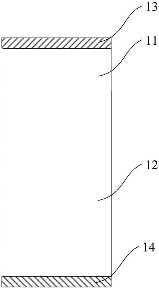
[0083] It should be noted that the P-type semiconductor material layer 21 can be located on the upper surface of the N-type semiconductor material layer 22 (such as figure 2 shown), can also be located on the lower surface of the N-type semiconductor material layer 22, and can also be embedded in the N-type semico...

Embodiment 2

[0100] The present invention also provides a semiconductor structure, such as Figure 7 to Figure 9 As shown, among them, Figure 7 It is a schematic diagram of a three-dimensional structure in which the shape of the PN junction is a cube, Figure 8 is a schematic diagram of a three-dimensional structure in which the shape of the PN junction is a cylinder, Figure 9 for Figure 7 Schematic diagram of the cross-sectional structure; the structure of the semiconductor structure in this embodiment is roughly the same as that of the semiconductor structure described in Embodiment 1, the difference between the two is: in the semiconductor structure in Embodiment 1, each layer described The insulating material layers are stacked on the outside of the PN junction in turn, that is, the inner sides of the insulating material layers of each layer are in contact with the outer wall of the PN junction; and in this embodiment, the outer wall of the PN junction is in contact with the same ...

Embodiment 3

[0108] see Figure 14 and Figure 15 , the present invention also provides a semiconductor component, the semiconductor component includes a plurality of semiconductor structures as described in Embodiment 1 or Embodiment 2, Figure 14 and Figure 15 Taking multiple semiconductor structures as described in Embodiment 2 as an example, the semiconductor component can also be a structure comprising multiple semiconductor structures as described in Embodiment 1; multiple semiconductor structures are arranged in a line To form a parallel structure, that is, outer walls of insulating material layers of adjacent semiconductor structures are in contact with each other.


PUM


Abstract

The invention provides a semiconductor structure, a semiconductor assembly and a power semiconductor device. The semiconductor structure comprises a P-type semiconductor material layer, an N-type semiconductor material layer and multiple insulating material layers, wherein the N-type semiconductor material layer is adhered to the P-type semiconductor material layer, and forms a PN junction together with the P-type semiconductor material layer; the multiple insulating material layers are positioned on the outer side of the PN junction and are distributed along the laminated direction of the P-type semiconductor material layer and the N-type semiconductor material layer, and the relative dielectric constants of the adjacent insulting material layers are different. According to the semiconductor structure provided by the invention, the electric field distribution when the device is resistant to voltage is obviously optimized, and the breakdown voltage of the device is greatly improved; device voltage resistance drop caused by a junction edge electric field concentration effect is avoided, and pre-breakdown of the device is prevented; and a field ring and a metal field plate structure are avoided from being used, so that the chip area is decreased, the cost of the device is reduced, and the reliability of the device is improved.

Description

technical field [0001] The invention relates to the technical field of semiconductors, in particular to a semiconductor structure, a semiconductor component and a power semiconductor device. Background technique [0002] Power semiconductor diodes are the key components of circuit systems and the basis of power semiconductors. They are simple in structure and good in reliability, and are widely used in civil and military applications. In particular, wide bandgap semiconductor power diodes are especially suitable for high-voltage, high-power semiconductor power diodes due to their excellent characteristics such as large bandgap width, high critical breakdown electric field, high electron saturation velocity, good thermal conductivity, radiation resistance, and good chemical stability. It is one of the most potential power devices in power electronics applications. [0003] figure 1 It is a schematic diagram of a traditional diode structure in the prior art, mainly including...

Claims


Application Information

Patent Timeline
Patent Type & Authority Applications(China)
IPC IPC(8): H01L29/06H01L29/861
CPCH01L29/0615H01L29/8611H01L23/3185H01L23/3192H01L29/1095H01L29/7395H01L29/7802H01L29/861H01L29/06
Inventor 杜江锋李振超刘东白智元于奇李述洲
Owner UNIV OF ELECTRONICS SCI & TECH OF CHINA
Why Eureka
Try Eureka