A surface passivation method for crystalline silicon solar cells with adjustable charge density

A solar cell and charge density technology, applied in circuits, photovoltaic power generation, electrical components, etc., can solve the problem that the charge cannot be adjusted arbitrarily, and achieve the effects of easy upgrade, easy mass production, and small process changes

Active Publication Date: 2017-07-04
JIANGSU MICROVIA NANO EQUIP TECH CO LTD
View PDF1 Cites 0 Cited by
  • Summary
  • Abstract
  • Description
  • Claims
  • Application Information

AI Technical Summary

Problems solved by technology

For example, the patent number is 201380004255.9, titled multi-quantum well solar cell and solar cell manufacturing method, which discloses a manufacturing method of quantum well solar cell, which adopts the sputtering method to make quantum well nano-stacks. In addition, the above-mentioned The solar cell manufactured by the method, its charge cannot be adjusted arbitrarily

Method used


Image

  • A surface passivation method for crystalline silicon solar cells with adjustable charge density
  • A surface passivation method for crystalline silicon solar cells with adjustable charge density
  • A surface passivation method for crystalline silicon solar cells with adjustable charge density

Examples


Embodiment Construction

[0042] The specific embodiments of the present invention will be further described below in conjunction with the accompanying drawings.

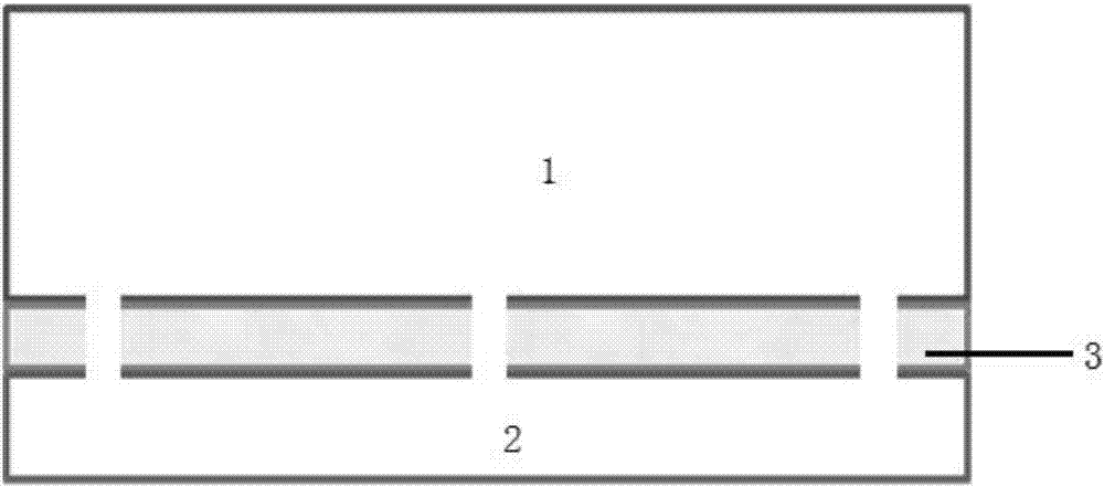
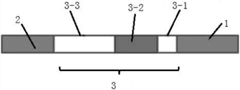
[0043] Such as figure 1 As shown, it is a schematic diagram of the position of the quantum well nano-stack in the solar cell, and the solar cell is provided with a quantum well nano-stack 3 between the silicon substrate 1 and the electrode 2 .

[0044] After the production steps of diffusion and etching, the laminated films required for quantum wells are deposited in one go by ALD. If the electrode material is opaque (such as metal), the quantum well stacked film structure is formed on the back of the battery (non-light-receiving surface). If the electrode material is transparent (such as a metal oxide transparent electrode), the quantum well stacked film structure can be formed on the front or back of the battery. After the film is plated, holes need to be opened on the film, and then the electrode material is plated to form a battery.

...


PUM


Abstract

The invention discloses a crystalline silicon solar cell surface passivation method capable of adjusting charge density. A quantum well structure is formed by a metal oxide nano laminated film on the surface of a crystalline silicon solar cell through an atomic layer deposition technology; a nano laminated layer of a quantum well comprises a tunneling layer, a trapping layer and a barrier layer in sequence; the thickness of the tunneling layer is 2-3nm, and the material is an oxide with a wide band gap; the thickness of the trapping layer is 3-6nm, and the material is the oxide with a narrow band gap; the thickness of the barrier layer is 5-10nm, and the material is the oxide with the wide band gap; and electrons are written into the trapping layer, a positive bias pulse needs to be applied to an electrode tip in the writing process, the voltage range is 6-15V and the voltage pulse is 100ns to 100ms. By the technical scheme, the method has the beneficial effects that the charge density in a passivation layer of the solar cell can be adjusted according to the writing voltage level and the time length of the pulse; and the density can be freely adjusted from 10<13>cm<-2> to 10<19>cm<-2> to achieve the optimum passivation effect.

Description

technical field [0001] The invention relates to the technical field of solar cell manufacturing, in particular to the surface passivation and antireflection technology of crystalline silicon cells for improving photoelectric conversion efficiency. Background technique [0002] Atomic Layer Deposition (ALD) technology is a nano-film deposition technology based on surface chemical vapor phase reaction. It can plate the substance on the surface of the substrate in the form of a monoatomic film, so the thickness and uniformity of the deposited film can be precisely controlled within the thickness of the atomic layer. Different from the traditional vacuum deposition technology, ALD technology has unique properties such as forming high-quality, pinhole-free and conformal thin films on the surface of non-planar complex structures and three-dimensional structures. At present, atomic layer deposition (ALD) technology, as one of the most advanced thin film deposition technologies, ha...

Claims


Application Information

Patent Timeline
Patent Type & Authority Patents(China)
IPC IPC(8): H01L31/18
CPCH01L31/1868Y02E10/50Y02P70/50
Inventor 李翔黎微明胡彬王燕清
Owner JIANGSU MICROVIA NANO EQUIP TECH CO LTD
Why Eureka
Try Eureka