GaN-based light-emitting diode epitaxial wafer and preparation method thereof

A light-emitting diode, gallium nitride-based technology, applied in electrical components, electric solid-state devices, circuits, etc., can solve the problems of limited improvement of antistatic properties and luminous efficiency of epitaxial wafers, and inability to release stress, and improve antistatic performance. and luminous efficiency, increase the probability of recombination, reduce the effect of leakage channels

Inactive Publication Date: 2016-11-16
HC SEMITEK ZHEJIANG CO LTD
View PDF4 Cites 18 Cited by
  • Summary
  • Abstract
  • Description
  • Claims
  • Application Information

AI Technical Summary

Problems solved by technology

[0004] However, InGaN shallow quantum wells can only reduce the lattice mismatch between the active layer and cannot release the stress formed before the growth of InGaN shallow quantum wells, and the antistatic properties and luminous efficiency of epitaxial wafers are very limited.

Method used


Image

  • GaN-based light-emitting diode epitaxial wafer and preparation method thereof
  • GaN-based light-emitting diode epitaxial wafer and preparation method thereof
  • GaN-based light-emitting diode epitaxial wafer and preparation method thereof

Examples


Embodiment Construction

[0025] In order to make the object, technical solution and advantages of the present invention clearer, the implementation manner of the present invention will be further described in detail below in conjunction with the accompanying drawings.

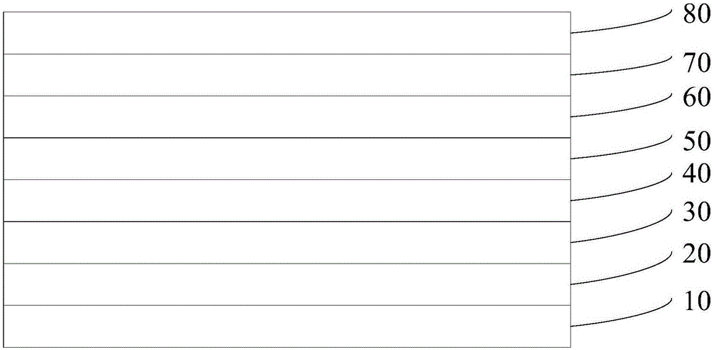
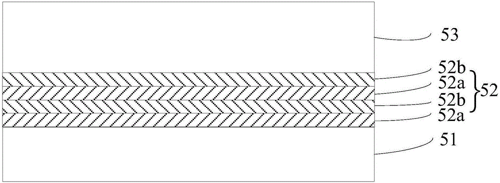
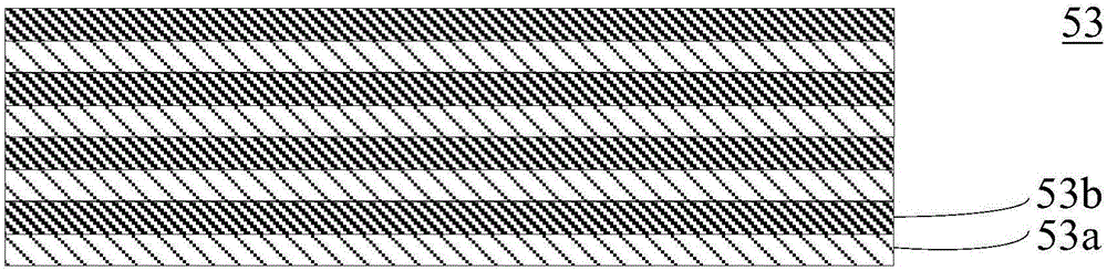
[0026] An embodiment of the present invention provides an epitaxial wafer of a gallium nitride-based light-emitting diode, figure 1 It is a structural diagram of an epitaxial wafer of a gallium nitride-based light-emitting diode provided by an embodiment of the present invention, as shown in figure 1 As shown, the epitaxial wafer includes a substrate 10, a buffer layer 20, an undoped GaN layer 30, an N-type contact layer 40, an active layer 60, a P-type electron blocking layer 70, and a P-type contact layer 80 stacked in sequence. The sheet also includes a stress release layer 50 interposed between the N-type contact layer 40 and the active layer 60, figure 2 is a structural diagram of a stress release layer provided by an embodiment...


PUM


Abstract

The invention discloses a GaN-based light-emitting diode epitaxial wafer and a preparation method thereof, and belongs to the technical field of photoelectron manufacture. The epitaxial wafer comprises a substrate, a buffer layer, a non-doped GaN layer, an N-type contact layer, a stress release layer, an active layer, a P-type electron blocking layer and a P-type contact layer. The stress release layer, comprising a first sublayer, a second sublayer and a third sublayer, is arranged between the N-type contact layer and the active layer, wherein the second sublayer comprises InxGa1-xN layers and N-type doped second GaN layers laminated alternatively, so that the stress formed due to lattice mismatch of a bottom layer can be effectively released, the piezoelectric polarization effect is reduced, and anti-static performance and luminous efficiency of the epitaxial wafer are improved. The first sublayer, the second sublayer and the third sublayer are N-type doped layers, thereby facilitating current expanding, reducing resistance at the two sides of the stress release layer and increasing capacitance at the two sides of the stress release layer; and more electrons are accumulated, so that a better electron blocking effect is achieved, electric leakage channels are reduced, and furthermore, the antistatic capability is further improved.

Description

technical field [0001] The invention relates to the field of optoelectronic manufacturing technology, in particular to an epitaxial wafer and a preparation method of a gallium nitride-based light-emitting diode. Background technique [0002] LED (Light Emitting Diode, Light Emitting Diode) has the advantages of small size, long life, low power consumption, etc., and is currently widely used in automobile signal lights, traffic signal lights, display screens and lighting equipment. [0003] During the growth process of epitaxial wafers of light-emitting diodes, stress often occurs due to lattice mismatch, resulting in poor crystal quality, decreased antistatic properties, and reduced luminous efficiency. In order to improve the antistatic properties and luminous efficiency of epitaxial wafers, a layer of InGaN shallow quantum wells is usually grown before growing the active layer to release the stress. [0004] However, InGaN shallow quantum wells can only reduce the lattice...

Claims


Application Information

Patent Timeline
Patent Type & Authority Applications(China)
IPC IPC(8): H01L33/12H01L33/14H01L23/60H01L33/00
CPCH01L33/12H01L23/60H01L33/007H01L33/14
Inventor 李红丽万林胡加辉
Owner HC SEMITEK ZHEJIANG CO LTD
Why Eureka
Try Eureka