Large-area single-crystal porous TiO2 thin film as well as preparation method and application thereof

A porous titanium dioxide, large-area technology, applied in the field of optoelectronic semiconductor materials, to achieve the effects of high controllability, high orientation, and high specific surface area

Active Publication Date: 2016-11-23
SUZHOU INST OF NANO TECH & NANO BIONICS CHINESE ACEDEMY OF SCI
View PDF5 Cites 7 Cited by
  • Summary
  • Abstract
  • Description
  • Claims
  • Application Information

AI Technical Summary

Problems solved by technology

Therefore, it is still a challenge to prepare a TiO thin film with high specific surface area and fast electron transport at the same time.

Method used


Image

  • Large-area single-crystal porous TiO2 thin film as well as preparation method and application thereof
  • Large-area single-crystal porous TiO2 thin film as well as preparation method and application thereof
  • Large-area single-crystal porous TiO2 thin film as well as preparation method and application thereof

Examples


preparation example Construction

[0035] In a typical embodiment of the present invention, a method for preparing a large-area single-crystal porous titanium dioxide film may comprise the following steps:

[0036] (1) The hydrothermal method is used to deposit TiO 2 A highly oriented porous titanium dioxide film is grown on the surface of the conductive substrate of the seed layer;

[0037] (2) Calcining the highly oriented porous titanium dioxide film obtained in step (1) to obtain a single crystal porous titanium dioxide film;

[0038] (3) Surface treatment and pore expansion treatment are performed on the single-crystal porous titanium dioxide film obtained in step (2), and large-area single-crystal porous titanium dioxide films with different pore sizes can be obtained.

[0039] In a more specific embodiment, a method for preparing a large-area single-crystal porous titanium dioxide film may comprise the following steps:

[0040] (1) Deposit TiO on the cleaned transparent conductive glass by dipping and ...

Embodiment 1

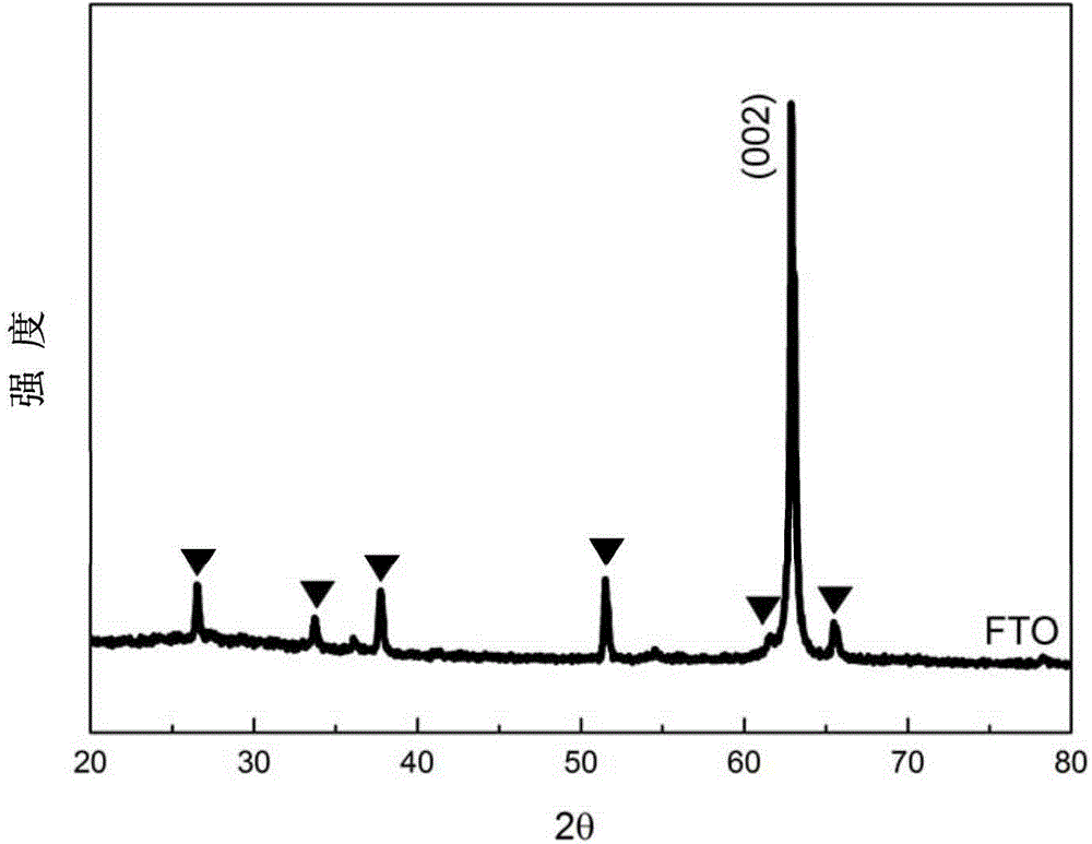
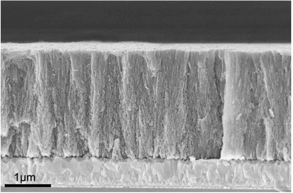
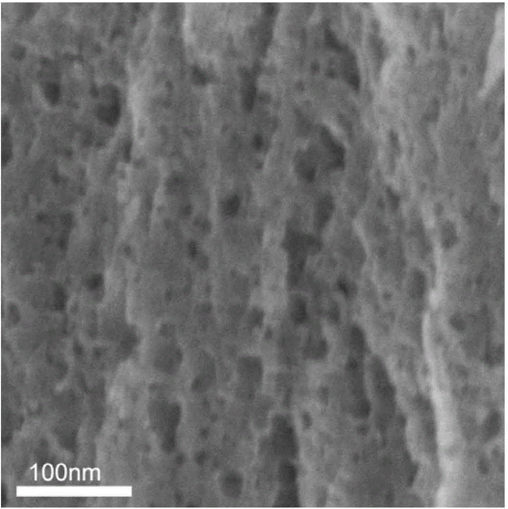
[0049] Example 1 will deposit TiO 2 The FTO glass of the seed layer (prepared by referring to the dipping and pulling method described above) was put into an autoclave, and 3.5mL of hydrochloric acid (37wt%), 0.16mL of sulfuric acid (96%), 8.3ml of deionized water and tetra-titanate Butyl ester 0.5mL, heat preservation at 180°C for 4h, take out the sample after cooling, rinse with deionized water and dry, then calcinate at 450°C for 30min in air atmosphere. Afterwards, the volume ratio of hydrogen peroxide and ammonia water was soaked for 20min in the mixed solution of 50:1, and it was taken out and rinsed with deionized water to obtain the final product, which was tested by XRD ( figure 1 ) analyzed as rutile phase TiO with good crystallinity 2 , from SEM( Figure 2a-2b ) and TEM ( image 3 ), it can be seen that the sample morphology is a porous film with a thickness of about 2.5 μm and a pore size ranging from 3 nm to 20 nm, while HRTEM ( Figure 4 ), it can be found th...

Embodiment 2

[0050] Example 2 will deposit TiO 2 The FTO glass of the seed layer (prepared by referring to the dipping and pulling method described above) was put into an autoclave, and 3.2mL of hydrochloric acid (37wt%), 0.27mL of sulfuric acid (96%), 8.5ml of deionized water and tetra-titanate Butyl ester 0.5mL, heat preservation at 180°C for 4h, take out the sample after cooling, rinse with deionized water and dry, then calcinate at 450°C for 30min in air atmosphere. Afterwards, the volume ratio of hydrogen peroxide and ammonia water was soaked in a mixed solution of 50:1 for 20 minutes, taken out and rinsed with deionized water to obtain the final product, whose structure and performance were similar to those of Example 1.


PUM

PropertyMeasurementUnit
thicknessaaaaaaaaaa

Abstract

The invention discloses a large-area single-crystal porous TiO2 thin film as well as a preparation method and an application thereof. The preparation method comprises steps as follows: a highly oriented porous TiO2 thin film grows on the surface of a conductive substrate with a deposited TiO2 crystal seed layer by adopting a hydrothermal method; the highly oriented porous TiO2 thin film is calcinated, and a single-crystal porous TiO2 thin film is obtained; preferably, the single-crystal porous TiO2 thin film can be subjected to surface treatment and pore-expanding treatment, and the large-area single-crystal porous TiO2 thin film with different pore sizes is obtained. The preparation method is simple to operate and low in cost and has better controllability, and the single-crystal porous TiO2 thin film has controllable thin film thickness and pore size, higher orientation, a high specific surface area and fewer crystal boundaries and defects and provides an effective electronic transmission channel, thereby further having high electronic transmission rate and being suitable for wide application in photoelectric devices such as photo-anodes of the photoelectric devices.

Description

technical field [0001] The invention relates to a preparation process of a titanium dioxide thin film material, in particular to a large-area single-crystal porous titanium dioxide thin film and a preparation method thereof, which can be applied to optoelectronic devices, such as photoanodes of optoelectronic devices, and belong to the field of optoelectronic semiconductor materials. Background technique [0002] Optoelectronic devices are widely used in energy, environment, military and other fields. Among them, the photoelectrode, as the core component of optoelectronic devices, has received extensive attention from scholars all over the world. There are two key factors in improving the performance of photoelectrodes: on the one hand, a high specific surface area is required to enhance the capture and collection of electrons; on the other hand, the photoelectrode is required to have a high electron transport rate to reduce the probability of electron-hole recombination. ...

Claims


Application Information

Patent Timeline
Patent Type & Authority Applications(China)
IPC IPC(8): C03C17/25
Inventor 封心建杨劼盛夏
Owner SUZHOU INST OF NANO TECH & NANO BIONICS CHINESE ACEDEMY OF SCI
Why Eureka
Try Eureka