
Chip bonding block manufacturing method and chip

A manufacturing method and soldering block technology, which is applied in semiconductor/solid-state device manufacturing, electrical components, electrical solid devices, etc., can solve problems such as electrochemical corrosion of chip soldering blocks, and achieve the effect of solving electrochemical corrosion and preventing corrosion

Inactive Publication Date: 2017-01-04
PEKING UNIV FOUNDER GRP CO LTD +1
View PDF4 Cites 4 Cited by
  • Summary
  • Abstract
  • Description
  • Claims
  • Application Information

AI Technical Summary

Problems solved by technology

[0005] In order to improve the problems existing in the prior art, the present invention provides a method for manufacturing chip pads to solve the problem of electrochemical corrosion of chip pads exposed to the air

Method used


Image

  • Chip bonding block manufacturing method and chip
  • Chip bonding block manufacturing method and chip
  • Chip bonding block manufacturing method and chip

Examples


Embodiment Construction

[0024] The present invention will be described in detail below in conjunction with the accompanying drawings and specific embodiments.

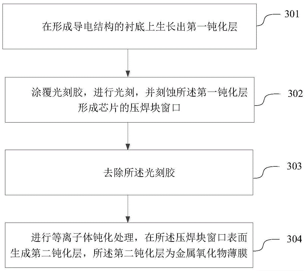
[0025] The invention provides a method for manufacturing chip pads, referring to the attached image 3 The process flow chart shown includes: step 301, growing a first passivation layer on the substrate forming the conductive structure; step 302, coating photoresist, performing photolithography, and etching the first passivation layer layer to form the pad window of the chip; step 303, remove the photoresist; step 304, perform plasma passivation treatment, and generate a second passivation layer on the surface of the pad window, and the second passivation The layer is a metal oxide film.

[0026] Wherein, the plasma passivation treatment is to place the chip in a dry debonding device that is fed with oxygen or a mixed gas of oxygen and inert gas.

[0027] Wherein, the removing the photoresist specifically includes: first placing the chip in...


PUM

PropertyMeasurementUnit
Thicknessaaaaaaaaaa

Abstract

The present invention discloses a chip bonding block manufacturing method and a chip. The method comprises: generating a first passivation layer on a substrate configured to form a conductive structure; coating photoresist, performing lithography and etching the first passivation layer to form the bonding block window of the chip; removing the photoresist; and performing plasma passivation processing, generating a second passivation layer at the surface of the bonding block window, wherein the second passivation layer is a metal oxide film, and the metal oxide film can prevent the chip bonding block from electrochemical corrosion through exposing in the air and cannot influence the subsequent packaging and routing. The present invention further discloses a chip, and the chip can prevent the bonding block from corrosion.

Description

technical field [0001] The invention relates to the field of semiconductor integrated circuit manufacturing, in particular to a method for manufacturing a chip bonding block and a chip. Background technique [0002] In the manufacturing process of integrated circuit chips, after all the front-end device manufacturing and back-end metal interconnection are completed, a passivation layer will be grown on the surface of the chip to prevent the metal lines from being mechanically damaged or corroded in subsequent steps. However, the pad portion of the chip must be exposed for testing and packaging. Since the pad window is not protected by any passivation layer, the metal is directly exposed in the air, and it is easy to react with water vapor in the air and impurity gases containing chlorine and fluorine in the subsequent process steps to cause surface corrosion, which will affect Chip performance even leads to wire bonding failure. Such as figure 1 It is an optical microscop...

Claims


Application Information

Patent Timeline
IPC IPC(8): H01L21/60H01L23/485
CPCH01L23/485H01L24/11H01L2224/11618
Inventor 石金成马万里高振杰崔永军汪龙强
Owner PEKING UNIV FOUNDER GRP CO LTD
Features
  • Generate Ideas
  • Intellectual Property
  • Life Sciences
  • Materials
  • Tech Scout
  • Unparalleled Data Quality
  • Higher Quality Content
  • 60% Fewer Hallucinations
Learn More