CIGS/CdTe dual-junction laminated thin-film solar cell and preparation method thereof

A solar cell and thin film technology, applied in circuits, photovoltaic power generation, electrical components, etc., can solve the problems of low utilization rate of the solar spectrum, loss, and the inability of photons to convert photogenerated carriers.

Active Publication Date: 2017-01-18
INST OF ELECTRICAL ENG CHINESE ACAD OF SCI
View PDF6 Cites 5 Cited by
  • Summary
  • Abstract
  • Description
  • Claims
  • Application Information

AI Technical Summary

Problems solved by technology

[0002] Conventional single-junction solar cells do not have a high utilization rate of the solar spectrum. Photons with photon energy greater than the bandwidth of the absorbing layer are absorbed and transformed into photogenerated carri

Method used


Image

  • CIGS/CdTe dual-junction laminated thin-film solar cell and preparation method thereof

Examples


preparation example Construction

[0039] The present invention provides a method for preparing a thin-film solar cell described in the above scheme, comprising the following steps:

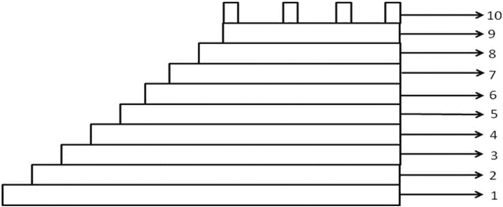
[0040] Prepare conductive electrodes, p-type CIGS absorber layer, bottom cell n-type CdS buffer layer, bottom cell intrinsic zinc oxide insulating layer, conductive connection layer, top cell intrinsic zinc oxide insulating layer, n-type CdS buffer on the substrate material layer, p-type CdTe absorber layer and copper-gold alloy electrode.

[0041] The present invention prepares conductive electrodes on the substrate material. In the present invention, the conductive electrode is preferably sputtered on the surface of the substrate by magnetron sputtering. In the present invention, the target material used in the magnetron sputtering is consistent with the above-mentioned scheme, and will not be repeated here; the diameter of the target is 75mm; the purity is preferably more than 99.99%; the magnetron sputtering The cathode magn...

Embodiment 1

[0084] Step 1: Prepare conductive electrodes by magnetron sputtering.

[0085] The Mo electrode is used as the conductive electrode, the target is a 3-inch forged fine-grained Mo target with a purity of 99.99%, the sputtering cathode magnetic field is an unbalanced field, and the back and bottom vacuum is pumped to 5.0×10 -3 Pa, the sputtering atmosphere is high-purity argon, the sputtering pressure is 0.1Pa, the sputtering power is 200W, the target base distance is 100mm, the sputtering time is 20min, and the thickness of the obtained Mo electrode is 800nm; The bottom surface is cleaned, the ion acceleration voltage is 250eV, the particle beam current is 80mA, and the cleaning time is 5min;

[0086] Step 2: Three-step co-evaporation method to deposit p-type CIGS absorber layer

[0087] Back vacuum to 5.0×10 -5 Pa, heat the bottom temperature, indium source, gallium source, and selenium source to 400°C, 800°C, 900°C, and 270°C respectively, wait for each evaporation source t...

Embodiment 2

[0108] Step 1: Preparation of conductive electrodes by magnetron sputtering

[0109] The Mo electrode is used as the conductive electrode, the target is a 3-inch forged fine-grained Mo target with a purity of 99.99%, the sputtering cathode magnetic field is an unbalanced field, and the back and bottom vacuum is pumped to 4.0×10 -3 Pa, the sputtering atmosphere is high-purity argon, the sputtering pressure is 0.5Pa, the sputtering power is 300W, the target base distance is 120mm, the sputtering time is 15min, and the thickness of the obtained Mo electrode is 1000nm; The bottom surface is cleaned, the ion acceleration voltage is 250eV, the particle beam current is 80mA, and the cleaning time is 5min;

[0110] Step 2: Three-step co-evaporation method to deposit p-type CIGS absorber layer

[0111] Back vacuum to 5.0×10 -5 Pa, heat the bottom temperature, indium source, gallium source, and selenium source to 450°C, 850°C, 950°C, and 300°C respectively, wait for each evaporation s...


PUM

PropertyMeasurementUnit
Thicknessaaaaaaaaaa
Thicknessaaaaaaaaaa
Thicknessaaaaaaaaaa

Abstract

The invention provides a CIGS/CdTe dual-junction laminated thin-film solar cell comprising a substrate, a CIGS bottom cell, a composite conductive layer and a CdTe top cell. The CIGS bottom cell consists of a cnductive electrode, a p type CIGS absorption layer and a bottom cell n type CdS buffer layer successively from bottom to top. The composite conductive layer includes a bottom cell intrinsic zinc-oxide insulating layer, a conductive connection layer and a top cell intrinsic zinc-oxide insulation layer of bottom cell successively from bottom to top. The CdTe top cell includes an N type CdS buffer layer, a p type CdTe absorbing layer and a copper gold alloy electrode successively from bottom to top. According to the invention, the narrow-band-gap bottom cell and the broad-band-gap top cell are connected by using the composite conductive layer to form a laminated cell, thereby improving the conversion efficiency of the thin-film cell. The experiment result demonstrates that the cell conversion efficiency of the CIGS/CdTe dual-junction laminated thin-film solar cell can reach 17.3%.

Description

technical field [0001] The invention relates to the technical field of a thin-film solar cell, in particular to a CIGS / CdTe double-junction stacked thin-film solar cell and a preparation method thereof. Background technique [0002] Conventional single-junction solar cells do not have a high utilization rate of the solar spectrum. Photons with photon energy greater than the bandwidth of the absorbing layer are absorbed and transformed into photogenerated carriers, but part of the energy of photons higher than the forbidden band width is lost in the form of phonon emission. Therefore, photons with photon energies smaller than the forbidden band width cannot be converted into photogenerated carriers. It is an important way to improve the conversion efficiency of solar cells by adopting multi-junction combinations of absorbing layers with different bandwidths to broaden the solar spectrum utilization range of the absorbing layer. The most successful development and production ...

Claims


Application Information

Patent Timeline
IPC IPC(8): H01L31/0445H01L31/032H01L31/0725H01L31/073H01L31/18
CPCH01L31/0322H01L31/0445H01L31/0725H01L31/073Y02E10/541Y02E10/543Y02P70/50
Inventor 屈飞李辉古宏伟丁发柱张贺
Owner INST OF ELECTRICAL ENG CHINESE ACAD OF SCI
Why Eureka
Try Eureka