Photoresist developer
A developing solution and photoresist technology, applied in optics, photography, opto-mechanical equipment, etc., can solve problems such as reduced developability, liquid crystal alignment problems, air bubbles, etc., to achieve less damage to fine patterns, and reduce residual and air bubbles. amount of effect
- Summary
- Abstract
- Description
- Claims
- Application Information
AI Technical Summary
Problems solved by technology
Method used
Image

Examples
Embodiment 1 to 8 and comparative example 1 to 4
[0052] Embodiment 1 to 8 and comparative example 1 to 4: the manufacture of photoresist developing solution
[0053] The components and contents described in the following Table 1 were mixed to prepare a photoresist developing solution. The remaining amount of water was added so that the total weight of the composition would be 100 parts by weight.
[0054] 【Table 1】
[0055]
[0056]
[0057] BPA-16: Add 16 moles of ethylene oxide to 1 mole of bisphenol A (SUNFOL BPA-16, SFC company)
[0058] BPA-18: Add 18 moles of ethylene oxide to 1 mole of bisphenol A (SUNFOL BPA-18, SFC Company)
[0059] DPA-14: Add 14 moles of ethylene oxide to 1 mole of 4,4'-methylene diphenol (SUNFOLDPA-14, SFC company)
[0060] BPA-20E2P: Add 20 moles of ethylene oxide and 2 moles of propylene oxide to 1 mole of bisphenol A (SUNFOL BPA-20E2P, SFC Company)
[0061] PCP-8: Add 8 moles of ethylene oxide (SUNFOL PCP-8, SFC company) to 1 mole of p-cumyl phenol (para-cumyl phenol)
[0062] MSP-9...
experiment example 1
[0068] Experimental example 1) Surfactant residual content analysis
[0069] On the glass substrate (100mm×100mm) used in the alkali-free TFT-LCD, negative photoresist (Red color photoresist, LED1R, LG Chemical Company) with a film thickness of 1.2-1.5 μm was spin-coated. Front exposure (42mJ / cm 2 ), the developing solutions involved in the respective examples and comparative examples in Table 1 above were diluted to 100 times with water. The substrate was treated with an aqueous ethanol solution having a concentration of 80% by weight, and after the surface of the color resist was extracted, the residual amount of the surfactant in the aqueous ethanol solution was measured by liquid chromatography.
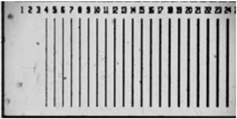
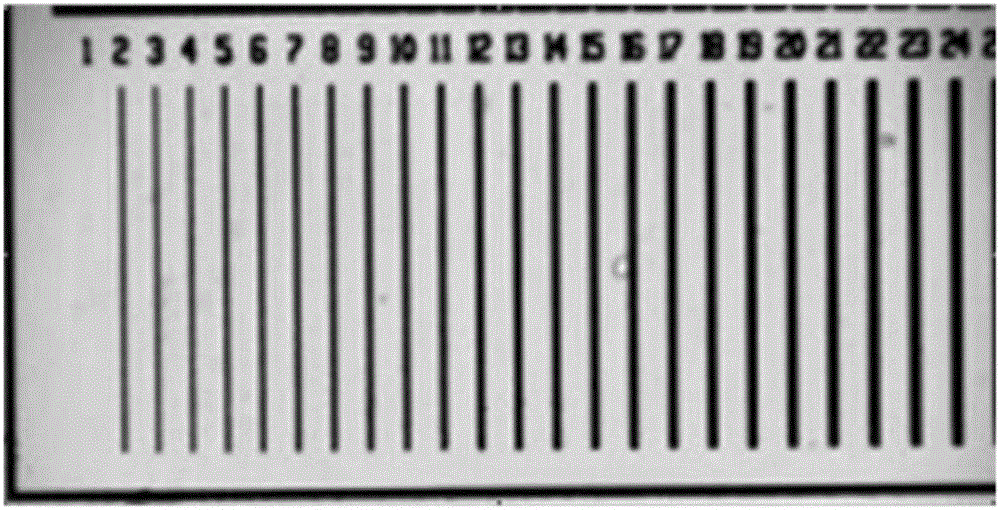
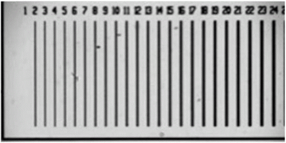
experiment example 2
[0070] Experimental Example 2) Confirmation of the photoresist pattern after development
[0071] On the glass substrate (100mm × 100mm) used in the alkali-free TFT-LCD, the negative photoresist (resin black matrix, TOK5110, TOK company) with a film thickness of 1.2-1.5 μm is spin-coated, and heated in an oven at 100 ° C A 100 second pre-bake was performed. Then use a pattern mask to expose (79mJ / cm 2 ), the developing solutions involved in the respective examples and comparative examples in Table 1 above were diluted to 100 times with water. After the developer treatment, it was washed with ultrapure water for a certain period of time, rinsed, air-dried with nitrogen, and then hard-baked in an oven at 220° C. for 20 minutes. The pattern of the photoresist with a width of 1 to 40 μm was observed with an optical microscope, and the degree of damage and loss of the pattern was confirmed.
PUM
| Property | Measurement | Unit |
|---|---|---|
| Thickness | aaaaa | aaaaa |
Abstract
Description
Claims
Application Information