
Method and apparatus for etching semiconductor substrate

A semiconductor and substrate technology, applied in the field of etching semiconductor substrates, can solve the problems of slow gas phase etching rate, loss of practical application value, poor etching uniformity, etc., to improve etching uniformity and avoid adhesion” effect of effect

Inactive Publication Date: 2017-02-15
INST OF MICROELECTRONICS CHINESE ACAD OF SCI
View PDF3 Cites 2 Cited by
  • Summary
  • Abstract
  • Description
  • Claims
  • Application Information

AI Technical Summary

Problems solved by technology

However, if there is no condensation layer, the gas phase etching rate will be too slow to lose practical application value, and the uniformity of etching will be poor.
[0006] Vapor-phase HF can effectively etch SiO 2 Thin film, but usually with other reaction by-products

Method used


Image

  • Method and apparatus for etching semiconductor substrate

Examples


Embodiment 1

[0039] This embodiment provides a method for etching a semiconductor substrate, and the method includes the following steps:

[0040] Step 101: converting the hydrofluoric acid liquid into hydrofluoric acid vapor, and converting the alcohol liquid into alcohol gas;

[0041] Step 102: Introduce the hydrofluoric acid vapor and the alcohol gas into the process chamber at the same time, the hydrofluoric acid vapor etches the substrate in the process chamber, and the alcohol gas acts as a moisturizing agent. The wet gas forms a uniform micro-condensation layer on the surface of the substrate. For example, hydrofluoric acid vapor is etching SiO 2 When the reaction product contains water, the alcohol gas in the process chamber and the surface of the substrate can be combined with water to prevent the formation of liquid water condensation phase on the surface of the substrate. The condensed water formed on the surface of the substrate will seriously affect the hydrofluoric acid. Et...

Embodiment 2

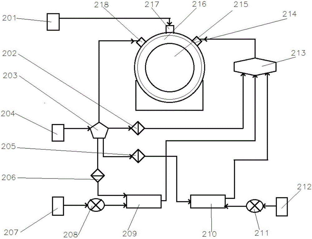
[0049] like figure 1 As shown, this embodiment provides a device for etching a semiconductor substrate, the device includes: a process chamber 216, a first pump 208, a first evaporator 209, a second pump 211, a second evaporator 210, a first A collection manifold and nozzles. Wherein, the process chamber 216 is used for placing the substrate 215, and the substrate 215 is subjected to an etching process in the process chamber 216; the first pump 208 pumps the hydrofluoric acid liquid into the first In the evaporator 209, the hydrofluoric acid liquid is partially converted into hydrofluoric acid vapor in the first evaporator 209; the second pump 211 pumps the alcohol liquid into the second evaporator 210, so The alcohol liquid is converted into alcohol gas in the second evaporator 210; the first collection manifold 203 is respectively connected to the first evaporator 209 and the second evaporator 210 through pipelines; nitrogen gas enters The first collection manifold 203 ent...


PUM


Abstract

The invention relates to the field of semiconductor and microelectromechanical system device manufacturing technology, and more particularly, to a method of etching a semiconductor substrate. The method comprises the steps of converting a hydrofluoric acid liquid into hydrofluoric acid vapor, and converting an alcohol liquid into an alcohol gas; and introducing the hydrofluoric acid vapor and the alcohol gas simultaneously into a process chamber, the hydrofluoric acid vapor etching the substrate in the process chamber, and the alcohol gas acting as a wetting gas to form a uniform micro-coagulation layer on the surface of the substrate. In order to achieve the above method, the invention also provides an apparatus for etching a semiconductor substrate. In the invention, an etching gas and a wetting gas are collectively introduced into the process chamber, the etching gas etches a substrate, the wetting gas forms a uniform micro-coagulation layer on the surface of the substrate, and the wetting gas in the process chamber and on the surface of the substrate can be combined with water to prevent the liquid water coagulation phase from forming on the surface of the substrate to improve the etching uniformity.

Description

technical field [0001] The invention relates to the technical field of semiconductor and micro-electromechanical system device manufacturing, in particular to a method and device for etching a semiconductor substrate. Background technique [0002] Epitaxial growth of Si, SiGe, TiSi 2 and Si 3 N 4 Before film deposition, in-situ SiO on the wafer surface needs to be 2 Just remove it. In some applications, such as Si epitaxial growth, high temperature baking is a method of removing in situ silicon oxide. However, in many cases a low temperature environment is required for processing because high temperatures may damage the structure of the device. In this case, wet immersion with HF chemical solution is generally used, but this HF solution immersion still has many disadvantages, such as removal of SiO 2 After that, the surface of the silicon wafer is hydrophobic, and the impurities in the HF solution are easily adsorbed on the surface to form pollution. [0003] Microele...

Claims


Application Information

Patent Timeline
Patent Type & Authority Applications(China)
IPC IPC(8): H01L21/306H01L21/67B81B7/02B81C1/00
CPCH01L21/306B81B7/02B81C1/00H01L21/30604H01L21/67H01L21/67063
Inventor 陈波夏洋李楠
Owner INST OF MICROELECTRONICS CHINESE ACAD OF SCI
Features
  • Generate Ideas
  • Intellectual Property
  • Life Sciences
  • Materials
  • Tech Scout
  • Unparalleled Data Quality
  • Higher Quality Content
  • 60% Fewer Hallucinations
Learn More