

A kind of preparation method of patterned fine conductive film
A conductive film and patterning technology, applied to the conductive layer on the insulating carrier, etc., can solve the problems of limited application fields, non-green and environmentally friendly etching process, and complicated processing process of the forming layer, so as to simplify the production process and low production efficiency , high cost effect
- Summary
- Abstract
- Description
- Claims
- Application Information
AI Technical Summary
Problems solved by technology
Method used
Image

Examples
Embodiment 1
[0062] Embodiment 1: Narrow frame touch screen.
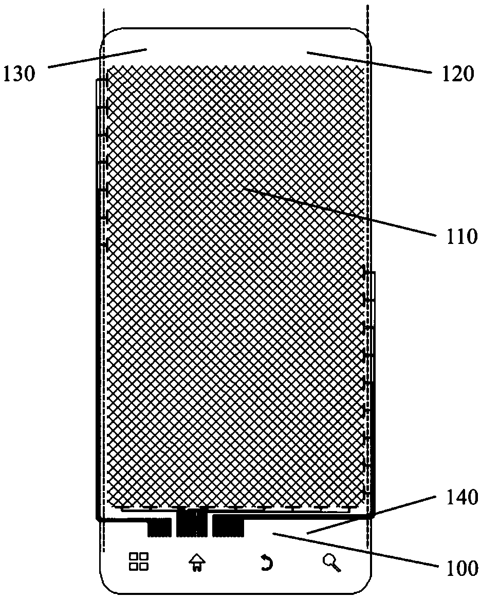
[0063] 1. Structure
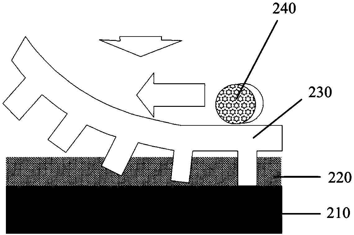
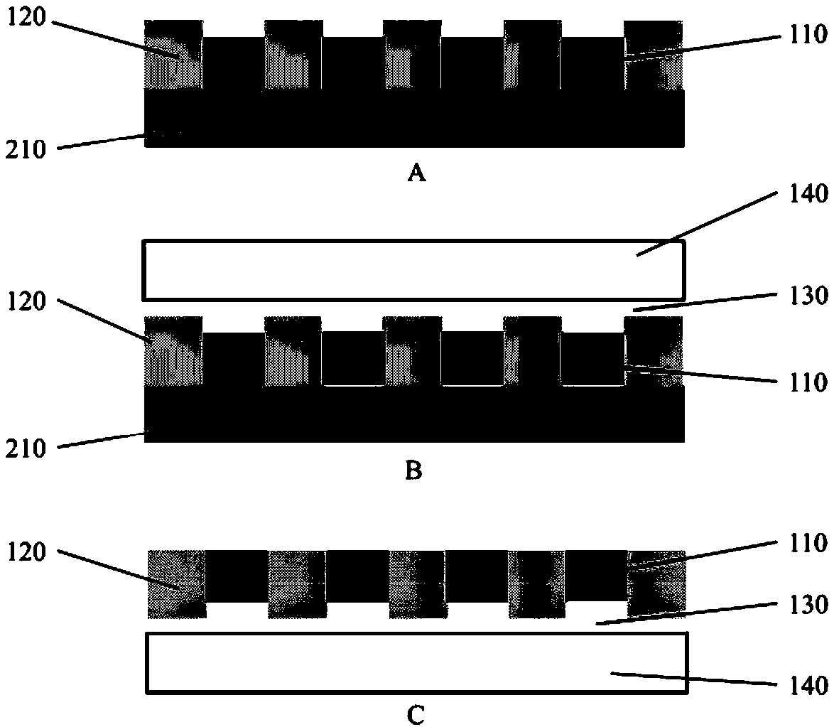
[0064] refer to figure 1 , the narrow frame touch screen in the preferred embodiment of the present invention includes a glass panel 100 , a pattern electrode 110 , an adhesive layer 120 , a cured adhesive layer 130 and a substrate layer 140 . The main part of the pattern electrode 110 is composed of a square grid, the thickness h of the grid is 1.5 microns, the line width d is 1.5 microns, and the side length of the grid square is 100 microns, which is composed of electrodeposited nickel wires. The pattern electrode 110 has a half-width of 1.5 microns and can be folded back to form a narrow frame touch screen. The glue layer 120 is an ultraviolet curable glue with a thickness of 1.8 microns. The cured glue layer 130 is a heat-curable or light-curable glue, and the material can be selected to be the same as that of the glue layer 120 . The substrate layer 140 can be a PET film with a light transmittance...
Embodiment 2
[0070] Embodiment 2, TFT array gate and storage capacitor in high-resolution LCD.
PUM
| Property | Measurement | Unit |
|---|---|---|
| surface roughness | aaaaa | aaaaa |
| particle diameter | aaaaa | aaaaa |
| width | aaaaa | aaaaa |
Abstract
Description
Claims
Application Information