Semiconductor structure forming method

A semiconductor and anti-penetration technology, applied in the direction of semiconductor devices, semiconductor/solid-state device manufacturing, electrical components, etc., can solve problems such as poor performance and serious short channel, and achieve short channel effect suppression, stable electrical performance, and device performance. stable effect

Active Publication Date: 2017-02-22
SEMICON MFG INT (SHANGHAI) CORP
View PDF3 Cites 11 Cited by
  • Summary
  • Abstract
  • Description
  • Claims
  • Application Information

AI Technical Summary

Problems solved by technology

[0004] However, as the size of semiconductor devices shrinks and the degree of integration increases, the feature size

Method used


Image

  • Semiconductor structure forming method
  • Semiconductor structure forming method
  • Semiconductor structure forming method

Examples


Embodiment Construction

[0032] As mentioned in the background art, as the size of semiconductor devices shrinks and the degree of integration increases, the feature size of FinFETs also shrinks accordingly, which makes the short channel of FinFETs increasingly serious and poor in performance.

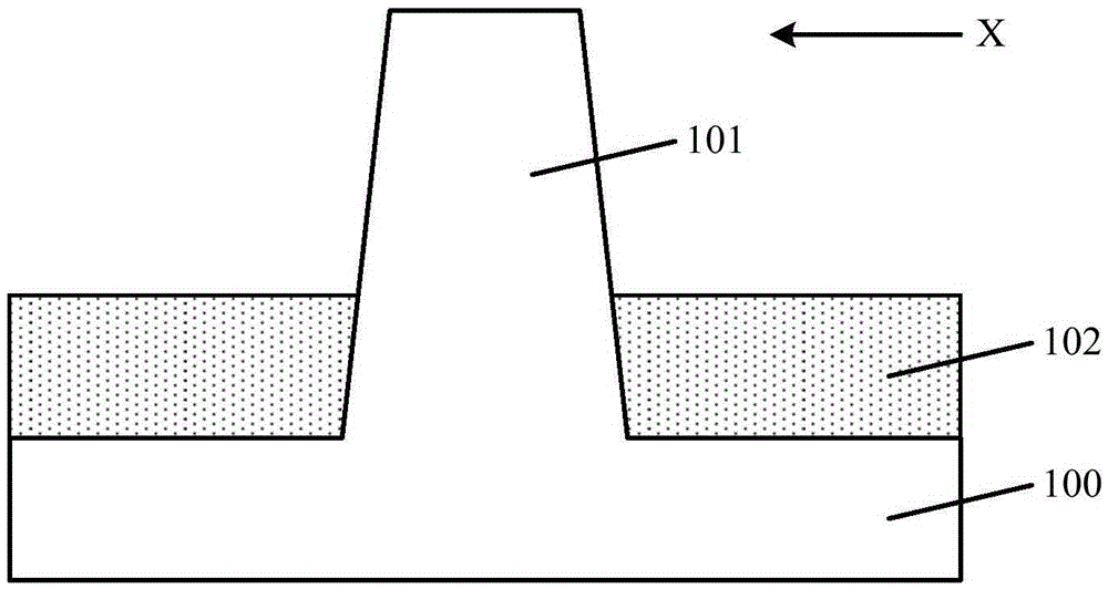
[0033] Please refer to figure 1 , figure 1 It is a schematic cross-sectional structure diagram of a fin for forming a fin field effect transistor according to an embodiment of the present invention, including: a substrate 100, a fin 101 located on the surface of the substrate 100, and an isolation layer 102 located on the surface of the fin 101. The isolation layer 102 covers part of the sidewall surface of the fin portion 101 , and the surface of the isolation layer 102 is lower than the top surface of the fin portion 101 .

[0034] Wherein, the base 100 and the fin 101 have well regions inside. When the FinFET is a PMOS transistor, the well is doped with N-type ions; when the FinFET is an NMOS transistor, ...


PUM


Abstract

The invention provides a semiconductor structure forming method which comprises the following steps: providing a substrate with a well region, wherein a first type of ions are disposed in the well region; using a first anti-punch-through-injection process to inject the first type of ion into the well region wherein the depth of the first anti- punch-through injection process is less than the distance from the bottom of the well region to the top surface of the substrate, forming an anti-punch-through region in the well region; using a second anti- punch-through-injection process to inject carbon ions into the well region to form a carbon doped region in the well region wherein the doped concentration of the carbon ions is greater than that of the first type of ion in the anti-punch-through region and the carbon doped region surrounds the anti-punch-through region; and using a third anti-punch-through-injection process to inject nitrogen ions into the well region wherein the third anti-punch-through-injection depth is less than those of the first anti- punch-through -injection and the second anti-punch-through-injection, forming a nitrogen doped region between the anti- punch-through regions and the top part of the substrate. According to the semiconductor structure forming method, it is possible to improve the performances of a semiconductor device.

Description

technical field [0001] The invention relates to the technical field of semiconductor manufacturing, in particular to a method for forming a semiconductor structure. Background technique [0002] With the rapid development of semiconductor manufacturing technology, semiconductor devices are developing towards higher element density and higher integration. As the most basic semiconductor device, transistors are currently being widely used. Therefore, with the increase of component density and integration of semiconductor devices, the gate size of planar transistors is getting shorter and shorter. The ability of traditional planar transistors to control channel current Weakened, resulting in short channel effect, resulting in leakage current, and ultimately affecting the electrical performance of semiconductor devices. [0003] In order to overcome the short-channel effect of the transistor and suppress the leakage current, a Fin Field Effect Transistor (Fin FET) is proposed i...

Claims


Application Information

Patent Timeline
IPC IPC(8): H01L21/336H01L21/265H01L29/78
CPCH01L29/66795H01L21/26506H01L29/785
Inventor 李勇
Owner SEMICON MFG INT (SHANGHAI) CORP
Why Eureka
Try Eureka