
High efficiency silicon-based heterojunction double-sided battery and its preparation method

A double-sided cell and heterojunction technology, applied in the field of solar cells, can solve the problems of reducing the photoelectric conversion efficiency of the cell, that is, the output power, and reducing the short-circuit current of the cell, so as to increase the photoelectric conversion efficiency, improve the electrical performance, and reduce the recombination Effect

Active Publication Date: 2017-02-22
GOLD STONE (FUJIAN) ENERGY CO LTD
View PDF4 Cites 3 Cited by
  • Summary
  • Abstract
  • Description
  • Claims
  • Application Information

AI Technical Summary

Problems solved by technology

Due to the high self-built electric field, it is easier to separate the carriers generated in the PN junction and in the crystalline silicon, that is, electrons and holes. However, due to the diffusion of electrons, electrons will also move to the emitter, resulting in electrons and holes being separated. The recombination of the emitter region reduces the short-circuit current of the cell and reduces the photoelectric conversion efficiency of the cell, that is, the output power

Method used


Image

  • High efficiency silicon-based heterojunction double-sided battery and its preparation method
  • High efficiency silicon-based heterojunction double-sided battery and its preparation method
  • High efficiency silicon-based heterojunction double-sided battery and its preparation method

Examples


Embodiment 1

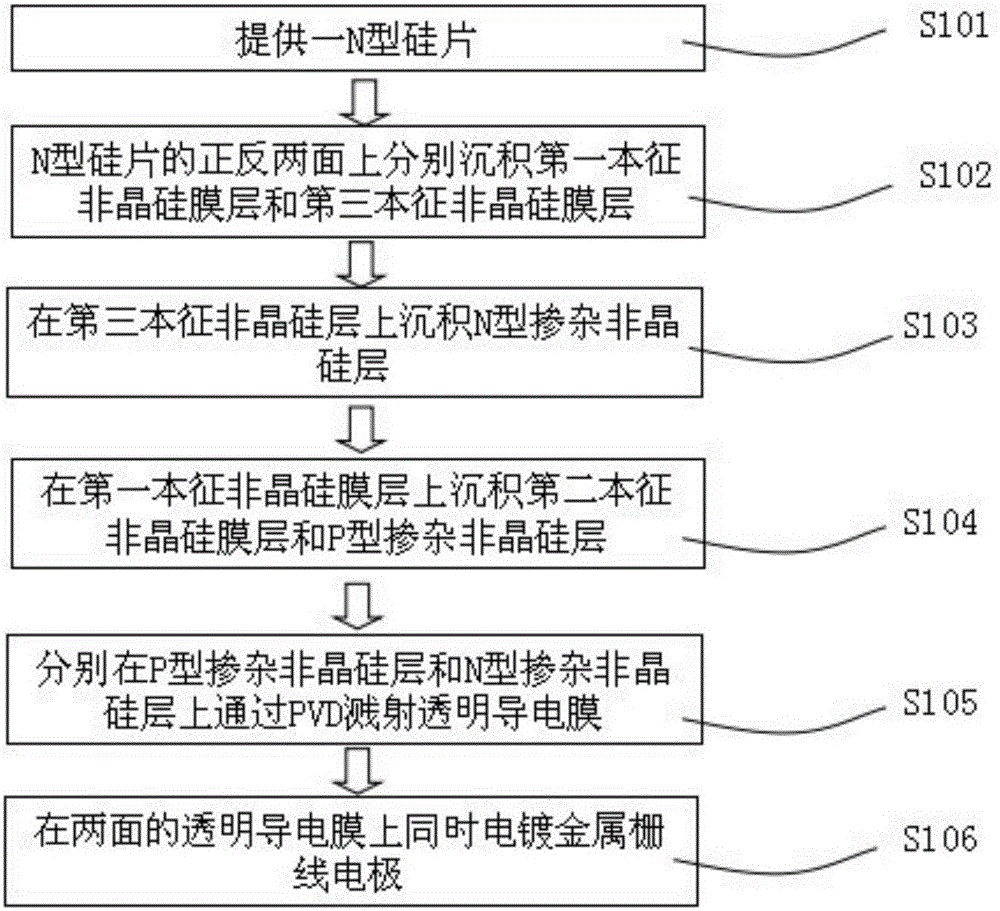
[0030] Such as figure 2 As shown, the invention discloses a method for preparing a high-efficiency silicon-based heterojunction double-sided battery, which includes the following steps:

[0031] S101: providing an N-type silicon wafer;

[0032] S102: Under the first temperature condition, respectively deposit a first intrinsic amorphous silicon film layer and a third intrinsic amorphous silicon film layer by chemical vapor deposition on both sides of the N-type silicon wafer;

[0033] S103: Depositing an N-type doped amorphous silicon layer on the third intrinsic amorphous silicon layer;

[0034] S104: Depositing a second intrinsic amorphous silicon film layer and a P-type doped amorphous silicon layer on the first intrinsic amorphous silicon film layer under a second temperature condition;

[0035] S105: Depositing a transparent conductive film on the P-type doped amorphous silicon layer and the N-type doped amorphous silicon layer by PVD (Physical Vapor Deposition) magnetro...

Embodiment 2

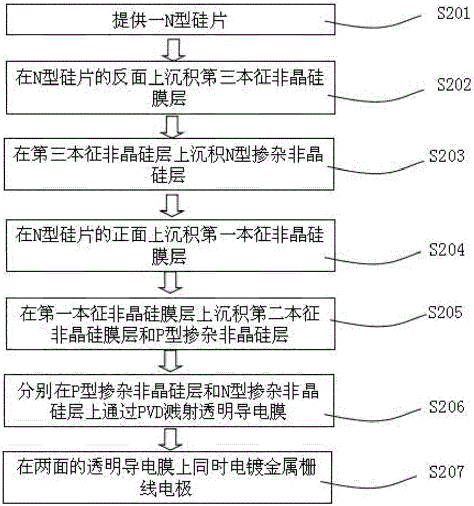
[0044] Such as image 3 As shown, the difference from Example 1 is that in this example, the third intrinsic amorphous silicon film layer and the N-type doped amorphous silicon layer on one side of the N-type silicon wafer are prepared first, and then another The first intrinsic amorphous silicon layer, the second intrinsic amorphous silicon layer and the P-type doped amorphous silicon layer on one side, and finally prepare a transparent conductive film layer and a metal grid line electrode, which specifically includes the following steps:

[0045] S201: providing an N-type silicon wafer;

[0046] S202: Under the first temperature condition, respectively deposit a third intrinsic amorphous silicon film layer on the reverse side of the N-type silicon wafer by chemical vapor deposition;

[0047] S203: depositing an N-type doped amorphous silicon layer on the third intrinsic amorphous silicon layer;

[0048] S204: respectively depositing a first intrinsic amorphous silicon film...

Embodiment 3

[0054] Such as Figure 4 As shown, the difference from Example 1 is that in this example, the first intrinsic amorphous silicon layer, the second intrinsic amorphous silicon layer and the P-type doped amorphous silicon layer on one side of the N-type silicon wafer are prepared first. crystalline silicon layer, and then prepare the third intrinsic amorphous silicon film layer and N-type doped amorphous silicon layer on the other side, and finally prepare a transparent conductive film layer and a metal grid line electrode, which specifically includes the following steps:

[0055] S301: providing an N-type silicon wafer;

[0056] S302: Depositing a first intrinsic amorphous silicon film layer on the front side of the N-type silicon wafer by chemical vapor deposition under the first temperature condition;

[0057] S303: Depositing a second intrinsic amorphous silicon film layer and a P-type doped amorphous silicon layer on the first intrinsic amorphous silicon film layer under a ...


PUM

PropertyMeasurementUnit
Thicknessaaaaaaaaaa
Thicknessaaaaaaaaaa
Thicknessaaaaaaaaaa

Abstract

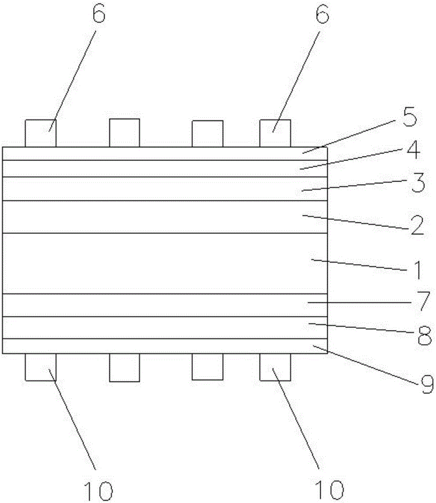
The invention discloses a high efficiency silicon-based heterojunction double-sided battery and its preparation method. The high efficiency silicon-based heterojunction double-sided battery comprises an N type silicon chip. On the front side of the N type silicon chip, a first intrinsic amorphous silicon layer, a second intrinsic amorphous silicon layer, a P type doped amorphous silicon layer, a transparent conductive film layer and a metal gate wire electrode are arranged in succession. The electron band gap of the second intrinsic amorphous silicon layer is greater than that of the first intrinsic amorphous silicon layer. On the back side of the N type silicon chip, a third intrinsic amorphous silicon layer, an N type doped amorphous silicon layer, a transparent conductive film layer and a metal gate wire electrode are arranged in succession. According to the invention, the first intrinsic amorphous silicon layer and the second intrinsic amorphous silicon layer are prepared in different chambers respectively, and the preparation temperature of the first intrinsic amorphous silicon layer is lower than that of the second intrinsic amorphous silicon layer so that the second intrinsic amorphous silicon layer has a relatively wider electron band gap which corresponds to the band gap of a crystalline silicon and therefore, can be used as a barrier layer to block the diffusion of electrons into the emitter using the difference in band width; therefore, the combination of electrons with empty cavities can be reduced, improving the electrical performance of the battery.

Description

technical field [0001] The invention relates to the field of solar cells, in particular to a high-efficiency silicon-based heterojunction double-sided cell and a preparation method thereof. Background technique [0002] A thin film solar cell is a solar cell formed by depositing a thin photoelectric material on a substrate. Thin-film solar cells can still generate electricity under weak light conditions, and their production process consumes less energy, which has the potential to greatly reduce raw material and manufacturing costs. Therefore, the market demand for thin-film solar cells is gradually increasing, and thin-film solar cell technology has become a research hotspot in recent years. Among them, improving photoelectric conversion efficiency and reducing costs are the ultimate goals of the solar industry. [0003] Silicon-based solar cells have become more attractive in recent years as the cost of the silicon material has decreased. To improve the conversion effic...

Claims


Application Information

Patent Timeline
IPC IPC(8): H01L31/0747H01L31/20
CPCH01L31/0747H01L31/202Y02E10/50Y02P70/50
Inventor 杨与胜王树林宋广华庄辉虎
Owner GOLD STONE (FUJIAN) ENERGY CO LTD
Learn More