Insulator possessing hole microgroove texturing surface and manufacturing method thereof
An insulator and textured technology is applied in the field of insulators with a textured surface of holes and microgrooves and the field of preparation thereof, which can solve the problems of difficulty in meeting the vacuum insulation requirements of high-voltage devices, low surface breakdown voltage resistance of insulators, and low reliability. , to achieve the effect of easy control, less influencing factors, and inhibition of multiplication
- Summary
- Abstract
- Description
- Claims
- Application Information
AI Technical Summary
Problems solved by technology
Method used
Image
Examples
Embodiment 1
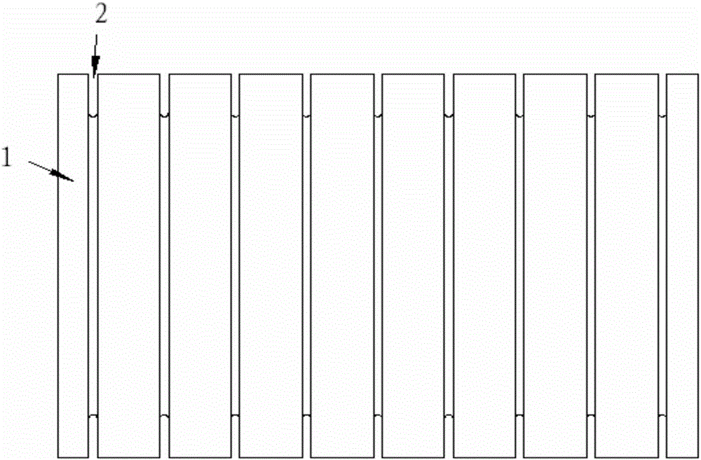
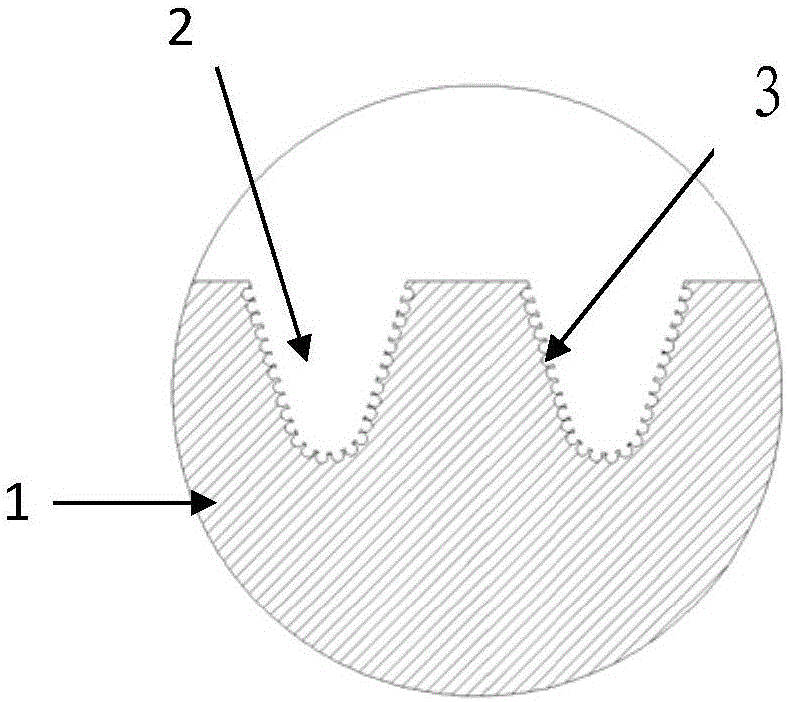
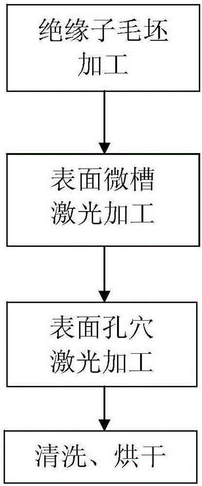
[0040] see figure 1 , figure 2 , at room temperature, according to image 3 The flow chart shown carries out the surface texturing process of polymer insulators. Firstly, the machined plexiglass (polymethyl methacrylate) cylindrical insulator body 1 with a diameter of 40 mm and a height of 10 mm is cleaned and installed on a rotary table. Secondly, a carbon dioxide laser with a wavelength of 10640nm is used, the pulse frequency is set to 150kHz, the power is 30W, the scanning rate of the laser beam is 50mm / s, and the number of scanning is 5 times. Focus the light beam on the surface of the material, and carve an array of parallel linear microgrooves 2 in the center of the material, wherein a single microgroove 2 has a width of 150 microns, a depth of 100 microns, and a spacing of 50 microns; The shortest distance between them is 1mm, and there are 40 parallel micro-groove rings in total. Again, choose a carbon dioxide laser with a wavelength of 10640nm, set the laser powe...
Embodiment 2
[0042] At room temperature, clean the machined epoxy resin cylindrical insulator body with a diameter of 40 mm and a height of 10 mm, and install it on a rotary table. A fiber laser with a wavelength of 1064nm is used, the pulse frequency is set to 100kHz, the power is 20W, the scanning rate of the laser beam is 30mm / s, and the number of scanning is 3 times. Focus the light beam on the surface of the material, and carve an array of parallel linear microgrooves in the center of the material. Among them, the width of a single microgroove is 80 microns, the depth is 100 microns, and the spacing is 80 microns; the shortest distance between the microgroove array and the end face of the cylinder is 1 mm, and a total of 50 parallel microgroove rings are formed. After the engraving is completed, reduce the laser power to 3W, and perform hole-making treatment on the surface of the microgroove. A three-dimensional profilometer is used to measure the profile of the microgroove and the s...
PUM
| Property | Measurement | Unit |
|---|---|---|
| width | aaaaa | aaaaa |
| depth | aaaaa | aaaaa |
| width | aaaaa | aaaaa |
Abstract
Description
Claims
Application Information


